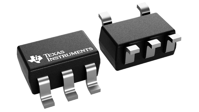
Packaging information
| Package | Pins SOT-SC70 (DCK) | 5 |
| Operating temperature range (°C) -40 to 125 |
| Package qty | Carrier 3,000 | LARGE T&R |
Features for the OPA838
- Gain bandwidth product: 300 MHz
- Very-low (trimmed) supply current: 950 µA
- Bandwidth: 90 MHz (A V = 6 V/V)
- High full-power bandwidth: 45 MHz, 4 V PP
- Negative rail input, rail-to-rail output
- Single-supply operating range: 2.7 V to 5.4 V
- 25°C input offset: ±125 µV (maximum)
- Input offset voltage drift: < ±1.6 µV/°C (maximum)
- Input voltage noise: 1.8 nV/√Hz (> 200 Hz)
- Input current noise: 1 pA/√Hz (> 2000 Hz)
- < 1-µA shutdown current for power savings
Description for the OPA838
The OPA838 decompensated voltage-feedback operational amplifier provides a high 300-MHz gain bandwidth product with 1.8-nV/√Hz input noise voltage, requiring only a trimmed 0.95-mA supply current. These features combine to provide an extremely power-efficient device for photodiode transimpedance designs and high-voltage gain stages, which require the lowest input voltage noise in signal receiver applications.
Operating at the minimum recommended noninverting gain of 6 V/V results in a 90-MHz, –3-dB bandwidth. Extremely low input noise and offset voltage make the OPA838 an excellent choice for high gains. Even at a dc-coupled gain of 1000 V/V, a 300-kHz signal bandwidth is available with a maximum output offset voltage of ±125 mV.
The single-channel OPA838 is available in 6-pin SOT-23 and SC70 packages with a power shutdown feature and a 5-pin SC70 package.