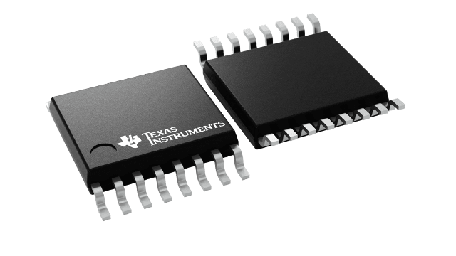
Packaging information
| Package | Pins TSSOP (PW) | 16 |
| Operating temperature range (°C) -40 to 85 |
| Package qty | Carrier 90 | TUBE |
Features for the SN74CB3T3257
- Output voltage translation tracks VCC
- Supports mixed-mode signal
operation on all data I/O ports
- 5V input down to 3.3V output level shift with 3.3V VCC
- 5V/3.3V input down to 2.5V output level shift with 2.5V VCC
- 5V-tolerant I/Os with device powered up or powered down
- Bidirectional data flow with near-zero propagation delay
- Low ON-state resistance (ron) characteristics (ron = 5Ω typ)
- Low input/output capacitance minimizes loading (Cio(OFF) = 5pF typ)
- Data and control inputs provide undershoot clamp diodes
- Low power consumption (ICC = 20µA max)
- VCC operating range from 2.3V to 3.6V
- Data I/Os support 0V to 5V signaling levels (0.8V, 1.2V, 1.5V, 1.8V, 2.5V, 3.3V, 5V)
- Control inputs can be driven by TTL or 5V/3.3V CMOS outputs
- Ioff supports partial-power-down mode operation
- Latch-up performance exceeds 250mA per JESD 17
- ESD performance tested per JESD
22
- 2000V human-body model (A114B, Class II)
- 1000V charged-device model (C101)
Description for the SN74CB3T3257
The SN74CB3T3257 is a high-speed TTL-compatible FET multiplexer/demultiplexer with low ON-state resistance (ron), allowing for minimal propagation delay. The device fully supports mixed-mode signal operation on all data I/O ports by providing voltage translation that tracks VCC. The SN74CB3T3257 supports systems using 5V TTL, 3.3V LVTTL, and 2.5V CMOS switching standards, as well as user-defined switching levels.
This device is fully specified for partial-power-down applications using Ioff. The Ioff feature verifies that damaging current does not backflow through the device when the device is powered down. The device has isolation during power off.
