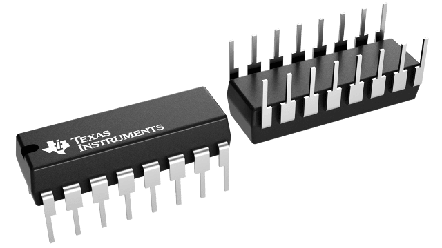
Packaging information
| Package | Pins PDIP (N) | 16 |
| Operating temperature range (°C) -40 to 125 |
| Package qty | Carrier 25 | TUBE |
Features for the SN74HC165
- Wide Operating Voltage Range of 2 V to 6 V
- Outputs Can Drive Up to 10 LSTTL Loads
- Low Power Consumption, 80-µA Maximum ICC
- Typical tpd = 13 ns
- ±4-mA Output Drive at 5 V
- Low Input Current of 1 µA Maximum
- Complementary Outputs
- Direct Overriding Load (Data) Inputs
- Gated Clock Inputs
- Parallel-to-Serial Data Conversion
- On Products Compliant to MIL-PRF-38535,
All Parameters Are Tested Unless Otherwise
Noted. On All Other Products, Production
Processing Does Not Necessarily Include Testing
of All Parameters.
Description for the SN74HC165
The SNx4HC165 devices are 8-bit parallel-load shift registers that, when clocked, shift the data toward a serial (QH) output. Parallel-in access to each stage is provided by eight individual direct data (A–H) inputs that are enabled by a low level at the shift/load (SH/LD) input. The SNx4HC165 devices also feature a clock-inhibit (CLK INH) function and a complementary serial (QH) output.
Clocking is accomplished by a low-to-high transition of the clock (CLK) input while SH/LD is held high and CLK INH is held low. The functions of CLK and CLK INH are interchangeable. Because a low CLK and a low-to-high transition of CLK INH also accomplish clocking, CLK INH must be changed to the high level only while CLK is high. Parallel loading is inhibited when SH/LD is held high. While SH/LD is low, the parallel inputs to the register are enabled independently of the levels of the CLK, CLK INH, or serial (SER) inputs.
