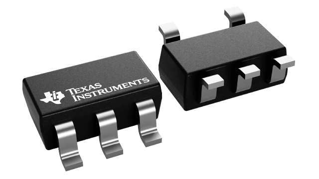
Packaging information
| Package | Pins SOT-23 (DBV) | 5 |
| Operating temperature range (°C) -40 to 125 |
| Package qty | Carrier 3,000 | LARGE T&R |
Features for the SN74LV1T04-Q1
-
AEC-Q100 qualified for automotive applications:
- Device temperature grade 1: -40°C to +125°C
- Device HBM ESD classification level 2
- Device CDM ESD classification level C4B
- Wide operating range of 1.8V to 5.5V
- Single-supply voltage translator (refer to
LVxT Enhanced Input Voltage):
- Up translation:
- 1.2V to 1.8V
- 1.5V to 2.5V
- 1.8V to 3.3V
- 3.3V to 5.0V
- Down translation:
- 5.0V, 3.3V, 2.5V to 1.8V
- 5.0V, 3.3V to 2.5V
- 5.0V to 3.3V
- Up translation:
- 5.5V tolerant input pins
- Supports standard pinouts
- Up to 150Mbps with 5V or 3.3V VCC
- Latch-up performance exceeds 250mAper JESD 17
Description for the SN74LV1T04-Q1
The SN74LV1T04-Q1 contains a single inverter gate with integrated voltage level translation. Each gate performs the Boolean function Y = A in positive logic. The output level is referenced to the supply voltage (VCC) and supports 1.8V, 2.5V, 3.3V, and 5V CMOS levels.
The input is designed with a lower threshold circuit to support up translation for lower voltage CMOS inputs (for example, 1.2V input to 1.8V output or 1.8V input to 3.3V output). In addition, the 5V tolerant input pins enable down translation (for example, 3.3V to 2.5V output).