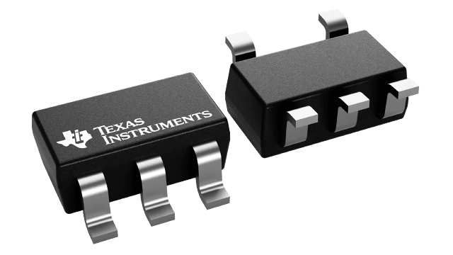
Packaging information
| Package | Pins SOT-23 (DBV) | 5 |
| Operating temperature range (°C) -40 to 125 |
| Package qty | Carrier 3,000 | LARGE T&R |
Features for the SN74LV1T34-Q1
-
AEC-Q100 qualified for automotive applications:
-
Device temperature grade 1: -40°C to +125°C
-
Device HBM ESD classification level 2
-
Device CDM ESD classification level C4B
-
-
Wide operating range of 1.8 V to 5.5 V
-
Single-supply voltage translator (refer to LVxT Enhanced Input Voltage):
-
Up translation:
-
1.2 V to 1.8 V
-
1.5 V to 2.5 V
-
1.8 V to 3.3 V
-
3.3 V to 5.0 V
-
-
Down translation:
- 5.0 V, 3.3 V, 2.5 V to 1.8 V
- 5.0 V, 3.3 V to 2.5 V
- 5.0 V to 3.3 V
-
- 5.5 V tolerant input pins
- Supports standard pinouts
- Up to 150 Mbps with 5 V or 3.3 V V CC
- Latch-up performance exceeds 250 mA per JESD 17
Description for the SN74LV1T34-Q1
The SN74LV1T34-Q1 contains a single buffer with extended voltage operation to allow for level translation. The buffer performs the Boolean function Y = A in positive logic. The output level is referenced to the supply voltage (V CC) and supports 1.8-V, 2.5-V, 3.3-V, and 5-V CMOS levels.
The input is designed with a lower threshold circuit to support up translation for lower voltage CMOS inputs (for example 1.2 V input to 1.8 V output or 1.8 V input to 3.3 V output). Additionally, the 5-V tolerant input pins enable down translation (for example 3.3 V to 2.5 V output).
