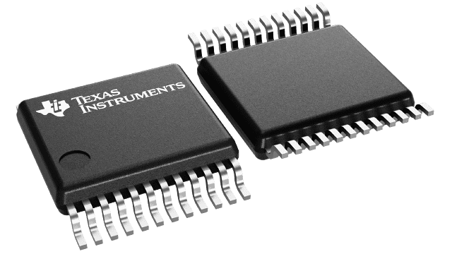
Packaging information
| Package | Pins TVSOP (DGV) | 24 |
| Operating temperature range (°C) -40 to 85 |
| Package qty | Carrier 2,000 | LARGE T&R |
Features for the SN74TVC3010
- Designed to be Used in Voltage-Limiting Applications
- 6.5-
 On-State Connection Between Ports A and B
 - Flow-Through Pinout for Ease of Printed Circuit Board Trace Routing
- Direct Interface With GTL+ Levels
- ESD Protection Exceeds JESD 22
- 2000-V Human-Body Model (A114-A)
- 1000-V Charged-Device Model (C101)
Description for the SN74TVC3010
The SN74TVC3010 provides 11 parallel NMOS pass transistors with a common gate. The low on-state resistance of the switch allows connections to be made with minimal propagation delay.
The device can be used as a 10-bit switch with the gates cascaded together to a reference transistor. The low-voltage side of each pass transistor is limited to a voltage set by the reference transistor. This is done to protect components with inputs that are sensitive to high-state voltage-level overshoots. (See Application Information in this data sheet.)
All of the transistors in the TVC array have the same electrical characteristics; therefore, any one of them can be used as the reference transistor. Since, within the device, the characteristics from transistor to transistor are equal, the maximum output high-state voltage (VOH) is approximately the reference voltage (VREF), with minimal deviation from one output to another. This is a large benefit of the TVC solution over discrete devices. Because the fabrication of the transistors is symmetrical, either port connection of each bit can be used as the low-voltage side, and the I/O signals are bidirectional through each FET.
