Packaging information
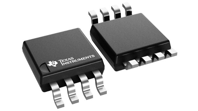
| Package | Pins VSSOP (DGK) | 8 |
| Operating temperature range (°C) -40 to 125 |
| Package qty | Carrier 2,500 | LARGE T&R |
Features for the TLV2365-Q1
- AEC-Q100 qualified
- Temperature grade 1: –40°C to +125°C
- Gain bandwidth: 50MHz
- Zero-crossover distortion topology:
- CMRR: 115dB (typical)
- Rail-to-rail input and
output
- Input 100mV beyond supply rail
- Noise: 4.5nV/√Hz
- Slew rate: 27V/µs
- Fast settling: 0.2µs to 0.01%
- Precision:
- Offset drift: 2.6µV/°C (maximum)
- Input bias current: 20pA (maximum)
- Operating voltage: 2.2V to 5.5V
Description for the TLV2365-Q1
The TLV365-Q1 and TLV2365-Q1 (TLVx365-Q1) devices are a family of zero-crossover, rail-to-rail input and output, CMOS operational amplifiers, optimized for low voltage and cost-sensitive applications. Low-noise (4.5nV/√Hz) and high-speed operation (50MHz gain bandwidth) make these devices an excellent choice for driving sampling analog-to-digital converters (ADCs) in applications such as low-side current sensing, audio, signal conditioning, and sensor amplification.
Special features include an excellent common-mode rejection ratio (CMRR), no input stage crossover distortion, high input impedance, and rail-to-rail input and output swing. The input common-mode range includes both the negative and positive supplies. The output voltage swings to within 12mV of the rails.
The TLVx365-Q1 are specified for operation from −40°C to +125°C.