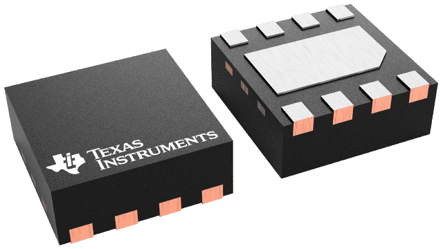
Packaging information
| Package | Pins WSON (DSG) | 8 |
| Operating temperature range (°C) -40 to 105 |
| Package qty | Carrier 3,000 | LARGE T&R |
Features for the TPS22975
- Integrated Single-Channel Load Switch
- Input Voltage Range: 0.6 V to VBIAS
- VBIAS Voltage Range: 2.5 V to 5.7 V
- On-Resistance (RON)
- RON = 16 mΩ (typical) at VIN = 0.6 V to 5.7 V,
VBIAS = 5.7 V
- RON = 16 mΩ (typical) at VIN = 0.6 V to 5.7 V,
- 6-A Maximum Continuous Switch Current
- Low Quiescent Current
- 37 µA (typical) at VIN = VBIAS = 5 V
- Low-Control Input-Threshold Enables Use of
1.2-, 1.8-, 2.5-, and 3.3-V Logic - Configurable Rise Time
- Thermal Shutdown
- Quick-Output Discharge (QOD) (Optional)
- SON 8-pin Package with Thermal Pad
- ESD Performance Tested per JESD 22
- 2000-V HBM and 1000-V CDM
Description for the TPS22975
The TPS22975 product family consists of two devices: TPS22975 and TPS22975N. Each device is a single-channel load switch that provides a configurable rise time to minimize inrush current. The device contains an N-channel MOSFET that can operate over an input voltage range of 0.6 V to 5.7 V and can support a maximum continuous current of 6 A. The switch is controlled by an on and off input (ON), which is capable of interfacing directly with low-voltage control signals. TPS22975 has an optional 230-Ω on-chip load resistor for quick output discharge when switch is turned off.
The TPS22975 is available in a small, space-saving 2-mm × 2-mm 8-pin SON package (DSG) with integrated thermal pad allowing for high power dissipation. The device is characterized for operation over the free-air temperature range of –40°C to +105°C.
