Packaging information
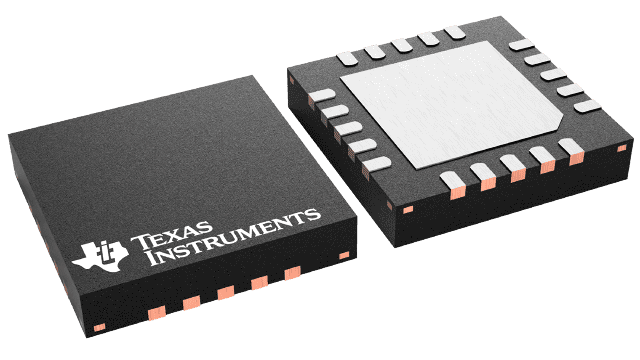
| Package | Pins WQFN (RTJ) | 20 |
| Operating temperature range (°C) -40 to 125 |
| Package qty | Carrier 250 | SMALL T&R |
Features for the TPS7A89
- Two Independent LDO Channels
- 4-mm × 4-mm, 20-Pin WQFN Package
- Low Output Noise: 3.8 µVRMS (10 Hz to 100 kHz)
- Low Dropout: 180 mV (typ) at 2 A
- Wide Input Voltage Range: 1.4 V to 6.5 V
- Wide Output Voltage Range: 0.8 V to 5.2 V
- High Power-Supply Rejection Ratio (PSRR):
- 75 dB at DC
- 40 dB at 100 kHz
- 40 dB at 1 MHz
- 1.0% Accuracy Over Line, Load, and Temperature
- Excellent Load Transient Response
- Adjustable Start-Up In-Rush Control
- Selectable Soft-Start Charging Current
- Independent Open-Drain Power-Good (PGx) Outputs
- Stable with a 10 µF or Larger Ceramic Output Capacitor
Description for the TPS7A89
The TPS7A89 is a dual, low-noise (3.8 µVRMS), low-dropout (LDO) voltage regulator capable of sourcing 2 A per channel with only 400 mV of maximum dropout.
The TPS7A89 provides the flexibility of two independent LDOs and approximately 60% smaller solution size than two single-channel LDOs. Each output is adjustable with external resistors from 0.8 V to 5.2 V. The wide input-voltage range of the TPS7A89 supports operation as low as 1.4 V and up to 6.5 V.
With 1% output voltage accuracy (over line, load, and temperature) and soft-start capabilities to reduce in-rush current, the TPS7A89 is ideal for powering sensitive analog low-voltage devices [such as voltage-controlled oscillators (VCOs), analog-to-digital converters (ADCs), digital-to-analog converters (DACs), high-end processors, and field-programmable gate arrays (FPGAs)].
The TPS7A89 is designed to power noise-sensitive components such as those found in high-speed communication, video, medical, or test and measurement applications. The very low 3.8-µVRMS output noise and wideband PSRR (40 dB at 1 MHz) minimizes phase noise and clock jitter. These features maximize the performance of clocking devices, ADCs, and DACs.