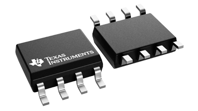
Packaging information
| Package | Pins SOIC (D) | 8 |
| Operating temperature range (°C) -40 to 125 |
| Package qty | Carrier 2,500 | LARGE T&R |
Features for the UCC5350
- Feature options
- Split outputs (UCC53x0S)
- UVLO referenced to GND2 (UCC53x0E)
- Miller clamp option (UCC53x0M)
- 8-pin D (4mm creepage) and DWV (8.5mm creepage) package
- 60ns (typical) propagation delay
- 100kV/µs minimum CMTI
- Isolation barrier life > 40 Years
- 3V to 15V input supply voltage
- Up to 33V driver supply voltage
- 8V and 12V UVLO options
- Negative 5V handling capability on input pins
- Safety-related certifications:
- 7000VPK isolation DWV (planned) and 4242VPK isolation D per DIN V VDE V 0884-11:2017-01 and DIN EN 61010-1
- 5000VRMS DWV and 3000VRMS D isolation rating for 1 minute per UL 1577
- CQC certification per GB4943.1-2011 D and DWV (planned)
- CMOS inputs
- Operating temperature: –40°C to +125°C
Description for the UCC5350
The UCC53x0 is a family of single-channel, isolated gate drivers designed to drive MOSFETs, IGBTs, SiC MOSFETs, and GaN FETs (UCC5350SBD). The UCC53x0S provides a split output that controls the rise and fall times individually. The UCC53x0M connects the gate of the transistor to an internal clamp to prevent false turn-on caused by Miller current. The UCC53x0E has its UVLO2 referenced to GND2 to get a true UVLO reading.
The UCC53x0 is available in a 4mm SOIC-8 (D) or 8.5mm SOIC-8 (DWV) package and can support isolation voltage up to 3kVRMS and 5kVRMS, respectively. With these various options the UCC53x0 family is a good fit for motor drives and industrial power supplies.
Compared to an optocoupler, the UCC53x0 family has lower part-to-part skew, lower propagation delay, higher operating temperature, and higher CMTI.
