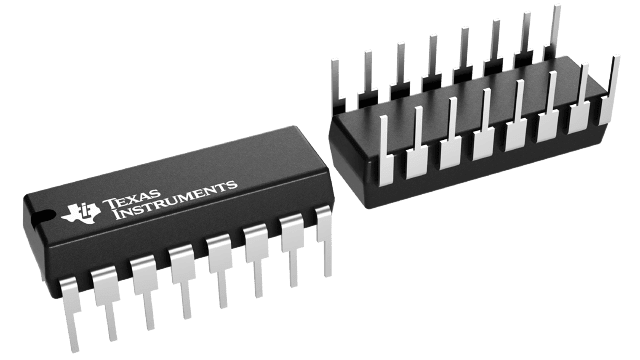
Gehäuseinformationen
| Gehäuse | Pins PDIP (N) | 16 |
| Betriebstemperaturbereich (°C) -55 to 125 |
| Gehäusemenge | Träger 25 | TUBE |
Merkmale von CD74HC4052
- Wide analog input voltage range: ±5V maximum
- Low ON-resistance:
- 70Ω typical (VCC – VEE = 4.5V)
- 40Ω typical (VCC – VEE = 9V)
- Low crosstalk between switches
- Fast switching and propagation speeds
- Break-before-make switching
- Wide operating temperature range: –40°C to +125°C
- Operation control voltage: 4.5V to 5.5V
- Switch voltage: 0V to 10V
- Direct LSTTL input logic compatibility VIL = 0.8V maximum, VIH = 2V minimum
- CMOS input compatibility II ≤ 1µA at VOL, VOH
Beschreibung von CD74HC4052
The CDx4HC405x and CDx4HCT405x device is a digitally controlled analog switch that uses silicon gate CMOS technology to achieve operating speeds similar to LSTTL with the low-power consumption of standard CMOS integrated circuits.
This analog multiplexer and demultiplexer controls analog voltages that may vary across the voltage supply range (for example, VCC to VEE). It is a bidirectional switch that allows any analog input to be used as an output and vice versa. The switch has low ON resistance and low OFF leakages. In addition, this device has an enable control that, when high, disables all switches to their OFF state.
