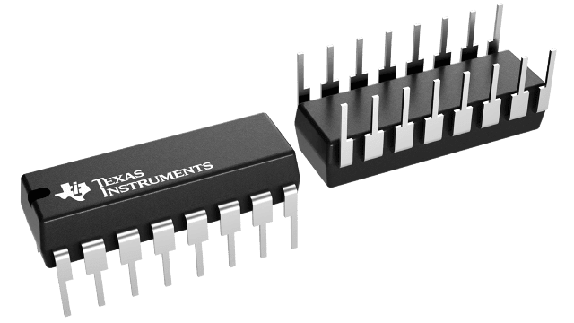
パッケージ情報
| パッケージ | ピン数 PDIP (N) | 16 |
| 動作温度範囲 (℃) -55 to 125 |
| パッケージ数量 | キャリア 25 | TUBE |
CD4028B の特徴
- BCD-to-decimal decoding or binary-to-octal decoding
- High decoded output drive capability
- "Positive logic" inputs and outputs……decoded outputs go high on selection
- Medium-speed operation… tPHL, tPLH = 80 ns (typ.) @ VDD = 10 V
- Standardized, symmetrical output characteristics
- 100% tested for quiescent current at 20 V
- Maximum input current of 1 µA at 18 V over full package-temperature range; 100 nA at 18 V and 25°C
- Noise margin (full package-temperature range) =
1 V at VDD = 5 V
2 V at VDD = 10 V
2.5 V at VDD = 15 V - 5-V, 10-V, and 15-V parametric ratings
- Meets all requirements of JEDEC Tentative Standard No. 13B, "Standard Specifications for Description of ’B’ Series CMOS Devices"
- Applications:
- Code conversion
- Indicator-tube decoder
- Address decoding-memory selection control
Data sheet acquired from Harris Semiconductor
CD4028B に関する概要
CD4028 types are BCD-to-decimal or binary-to-octal decoders consisting of buffering on all 4 inputs, decoding-logic gates, and 10 output buffers. A BCD code applied to the four input, A to D, results in a high level at the selected one of 10 decimal decoded outputs. Similarly, a 3-bit binary code applied to inputs A through C is decoded in octal code at output 0 to 7 if D = "0". High drive capability is provided at all outputs to enhance dc and dynamic performance in high fan-out applications.
The CD4028B-Series types are supplied in 16-lead hermetic dual-in-line ceramic packages (F3A suffix), 16-lead dual-in-line plastic packages (E suffix), 16-lead small-outline packages (M, M96, MT and NSR suffixes), and 16-lead thin shrink small-outline packages (PW and PWR suffixes).
