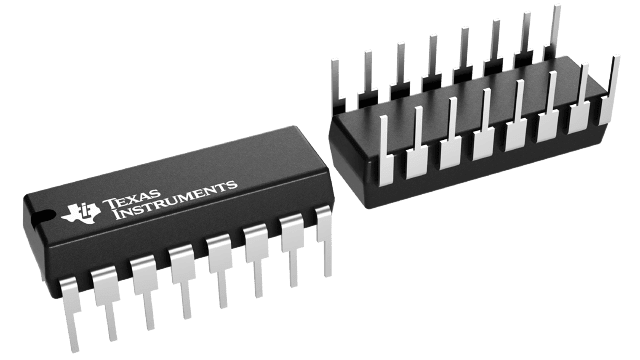
Packaging information
| Package | Pins PDIP (N) | 16 |
| Operating temperature range (°C) -55 to 125 |
| Package qty | Carrier 25 | TUBE |
Features for the CD4051B
- Wide range of digital and analog signal levels:
- Digital: 3V to 20V
- Analog: ≤ 20VP-P
- Single supply range : 3V to 20V (performance degrades for VDD < 3V)
- Dual Supply range: ± 3V to ± 10V
- Low ON resistance, 125Ω (typical) over input range for VDD = 15V
- Low channel leakage of ±10pA (typical) at VDD = 15V
- Low quiescent power dissipation : 0.2µW (typical)
- Break-before-make switching eliminates channel overlap
- Bidirectional signal path
- ESD protection HBM: 3000V, CDM: 2000V
- Pin compatible with industry standard 4051 muxes
Description for the CD4051B
The CD405xB analog multiplexers and demultiplexers are digitally-controlled analog switches having low ON impedance and very low OFF leakage current. These multiplexer circuits dissipate extremely low quiescent power over the full VDD – VSS and VDD – VEE supply-voltage ranges, independent of the logic state of the control signals.
