SBAS771D June 2017 – October 2024 AMC1303E0510 , AMC1303E0520 , AMC1303E2510 , AMC1303E2520 , AMC1303M0510 , AMC1303M0520 , AMC1303M2510 , AMC1303M2520
PRODUCTION DATA
- 1
- 1 Features
- 2 Applications
- 3 Description
- 4 Device Comparison Table
- 5 Pin Configuration and Functions
-
6 Specifications
- 6.1 Absolute Maximum Ratings
- 6.2 ESD Ratings
- 6.3 Recommended Operating Conditions
- 6.4 Thermal Information
- 6.5 Power Ratings
- 6.6 Insulation Specifications
- 6.7 Safety-Related Certifications
- 6.8 Safety Limiting Values
- 6.9 Electrical Characteristics: AMC1303x05x
- 6.10 Electrical Characteristics: AMC1303x25x
- 6.11 Switching Characteristics
- 6.12 Timing Diagrams
- 6.13 Insulation Characteristics Curves
- 6.14 Typical Characteristics
- 7 Detailed Description
- 8 Application and Implementation
- 9 Device and Documentation Support
- 10Revision History
- 11Mechanical, Packaging, and Orderable Information
Package Options
Mechanical Data (Package|Pins)
- DWV|8
Thermal pad, mechanical data (Package|Pins)
Orderable Information
8.2.2 Isolated Voltage Sensing
The AMC1303 is optimized for usage in current-sensing applications using low-resistance shunts. However, the device is also suitable for isolated voltage-sensing applications as long as the effect of the input bias current is considered. For best performance, use the ±250mV versions of the device (AMC1303x25xx) in this case.
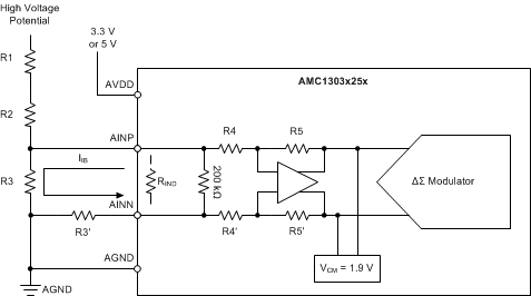
Figure 8-6 shows a simplified circuit typically used in high-voltage-sensing applications. The high value resistors (R1 and R2) are used as voltage dividers and dominate the current value definition. The resistance of the sensing resistor R3 is chosen to meet the input voltage range of the AMC1303. This resistor and the differential input resistance of the AMC1303x25x is 22kΩ also create a voltage divider that results in an additional gain error. With the assumption of R1, R2, and RIND having a considerably higher value than R3, the resulting total gain error is estimated using Equation 4, with EG being the gain error of the AMC1303.

This gain error is minimized during the initial system-level gain calibration procedure.
 Figure 8-6 Using the AMC1303x25x for Isolated Voltage Sensing