SBAS771D June 2017 – October 2024 AMC1303E0510 , AMC1303E0520 , AMC1303E2510 , AMC1303E2520 , AMC1303M0510 , AMC1303M0520 , AMC1303M2510 , AMC1303M2520
PRODUCTION DATA
- 1
- 1 Features
- 2 Applications
- 3 Description
- 4 Device Comparison Table
- 5 Pin Configuration and Functions
-
6 Specifications
- 6.1 Absolute Maximum Ratings
- 6.2 ESD Ratings
- 6.3 Recommended Operating Conditions
- 6.4 Thermal Information
- 6.5 Power Ratings
- 6.6 Insulation Specifications
- 6.7 Safety-Related Certifications
- 6.8 Safety Limiting Values
- 6.9 Electrical Characteristics: AMC1303x05x
- 6.10 Electrical Characteristics: AMC1303x25x
- 6.11 Switching Characteristics
- 6.12 Timing Diagrams
- 6.13 Insulation Characteristics Curves
- 6.14 Typical Characteristics
- 7 Detailed Description
- 8 Application and Implementation
- 9 Device and Documentation Support
- 10Revision History
- 11Mechanical, Packaging, and Orderable Information
Package Options
Mechanical Data (Package|Pins)
- DWV|8
Thermal pad, mechanical data (Package|Pins)
Orderable Information
7.3.3 Isolation Channel Signal Transmission
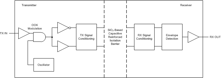
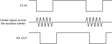
The AMC1303 uses an on-off keying (OOK) modulation scheme to transmit the modulator output bitstream across the capacitive SiO2-based isolation barrier. The transmitter modulates the bitstream at TX IN in Figure 7-3 with an internally generated, 480MHz carrier across the isolation barrier to represent a digital zero and sends a no signal to represent the digital one. The receiver demodulates the signal after advanced signal conditioning and produces the output. The symmetrical design of each isolation channel improves the CMTI performance and reduces the radiated emissions caused by the high-frequency carrier. Figure 7-3 shows a block diagram of an isolation channel integrated in the AMC1303.
 Figure 7-3 Block Diagram of an Isolation Channel
Figure 7-4 shows the concept of the on-off keying scheme.
 Figure 7-4 OOK-Based Modulation Scheme