SLVSDW6C April 2017 – April 2021 TPS7H1101A-SP
PRODUCTION DATA
- 1 Features
- 2 Applications
- 3 Description
- 4 Revision History
- 5 Pin Configuration and Functions
- 6 Specifications
- 7 Detailed Description
- 8 Application and Implementation
- 9 Power Supply Recommendations
- 10Layout
- 11Device and Documentation Support
- 12Mechanical, Packaging, and Orderable Information
Package Options
Mechanical Data (Package|Pins)
- HKR|16
- KGD|0
Thermal pad, mechanical data (Package|Pins)
Orderable Information
8.2.1.6 Current Sharing
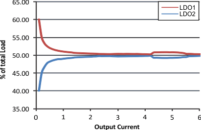
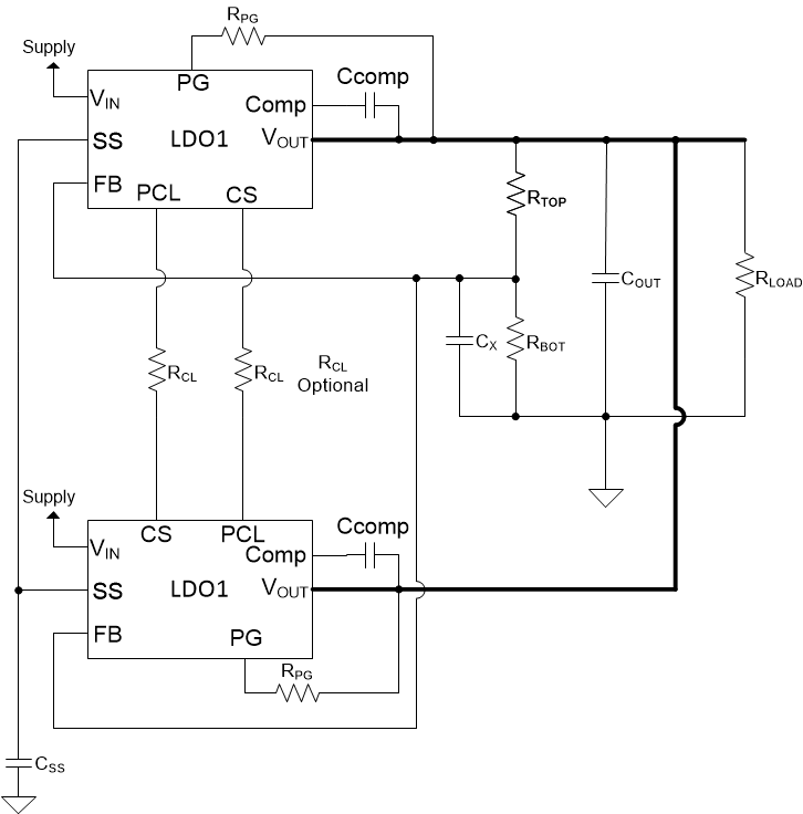
For demanding load requirements, multiple LDOs can be paralleled as indicated in Figure 8-12. In parallel mode, the CS terminal of LDO1 must be connected to the PCL terminal of LDO2 via a series resistor, RCL, and CS terminal of LDO2 must be connected to PCL terminal of LDO1 via series resistor, RCL. The typical value of RCL in parallel operation is 3.75 kΩ for current limit > 6 A. In parallel configuration, RCL (resistor from PCL to GND) and RCS (resistor from CS terminal to VIN) must be left open (unpopulated). The RCL value must be selected so that the operating condition of the CS terminal is maintained, as specified in Section 6.5. VCS must be greater than 0.3 V to insure proper current sense operation. The current from PCL through RCL of LDO1 is determined by the output load current of LDO2 divided by the CSR. Hence, the voltage at CS terminal of the LDO1 is 0.605 V – ((output load current of LDO2 + 0.2458) / CSR × RCL).
Alternately, it can also provide twice the output current to meet system needs. When using two LDOs in parallel operation for higher output load current, use POL TPS50601-SP as an input source.
 Figure 8-11 LDO Current Share
 Figure 8-12 Block Diagram (Parallel Operation)