JAJS253P April   2004  – August 2024 TPS2041B , TPS2042B , TPS2043B , TPS2044B , TPS2051B , TPS2052B , TPS2053B , TPS2054B

PRODUCTION DATA  

  1.   1
  2. 特長
  3. アプリケーション
  4. 概要
  5. General Switch Catalog
  6. Pin Configuration and Functions
  7. Specifications
    1. 6.1 Absolute Maximum Ratings
    2. 6.2 ESD Ratings
    3. 6.3 Recommended Operating Conditions
    4. 6.4 Thermal Information
    5. 6.5 Electrical Characteristics
    6. 6.6 Typical Characteristics (All Devices Excluding TPS2051BDBV and TPS2052BD)
    7. 6.7 Typical Characteristics (TPS2051BDBV and TPS2052BD)
  8. Parameter Measurement Information
  9. Detailed Description
    1. 8.1 Overview
    2. 8.2 Functional Block Diagrams
    3. 8.3 Feature Description
      1. 8.3.1  Power Switch
      2. 8.3.2  Charge Pump
      3. 8.3.3  Driver
      4. 8.3.4  Enable ( ENx)
      5. 8.3.5  Enable (ENx)
      6. 8.3.6  Current Sense
      7. 8.3.7  Overcurrent
        1. 8.3.7.1 Overcurrent Conditions (TPS20x3BD, TPS20x4BD, and TPS20x2BDRB)
        2. 8.3.7.2 Overcurrent Conditions (TPS20x1B & TPS20x2B in D, DGN, and DBV packages)
      8. 8.3.8  Overcurrent ( OCx)
      9. 8.3.9  Thermal Sense
      10. 8.3.10 Undervoltage Lockout
    4. 8.4 Device Functional Modes
  10. Application and Implementation
    1. 9.1 Application Information
      1. 9.1.1 Universal Serial Bus (USB) Applications
    2. 9.2 Typical Application
      1. 9.2.1 Typical Application (TPS2042B)
        1. 9.2.1.1 Design Requirements
        2. 9.2.1.2 Detailed Design Procedure
          1. 9.2.1.2.1 Power-Supply Considerations
          2. 9.2.1.2.2 OC Response
        3. 9.2.1.3 Application Curves
      2. 9.2.2 Host and Self-Powered and Bus-Powered Hubs
        1. 9.2.2.1 Design Requirements
          1. 9.2.2.1.1 USB Power-Distribution Requirements
        2. 9.2.2.2 Detailed Design Procedure
          1. 9.2.2.2.1 Low-Power Bus-Powered and High-Power Bus-Powered Functions
        3. 9.2.2.3 Application Curves
      3. 9.2.3 Generic Hot-Plug Applications
        1. 9.2.3.1 Design Requirements
        2. 9.2.3.2 Detailed Design Procedure
        3. 9.2.3.3 Application Curves
  11. 10Power Supply Recommendations
    1. 10.1 Undervoltage Lockout (UVLO)
  12. 11Layout
    1. 11.1 Layout Guidelines
    2. 11.2 Layout Example
    3. 11.3 Power Dissipation
    4. 11.4 Thermal Protection
  13. 12Device and Documentation Support
    1. 12.1 ドキュメントの更新通知を受け取る方法
    2. 12.2 サポート・リソース
    3. 12.3 Trademarks
    4. 12.4 静電気放電に関する注意事項
    5. 12.5 用語集
  14. 13Revision History
  15. 14Mechanical, Packaging, and Orderable Information
OC Response

The OCx open-drain output is asserted (active low) when an overcurrent or overtemperature shutdown condition is encountered after a 10-ms deglitch timeout. The output remains asserted until the overcurrent or overtemperature condition is removed. Connecting a heavy capacitive load to an enabled device can cause a momentary overcurrent condition; however, no false reporting on OCx occurs due to the 10-ms deglitch circuit. The TPS20xxB is designed to eliminate false overcurrent reporting. The internal overcurrent deglitch eliminates the need for external components to remove unwanted pulses. OCx is not deglitched when the switch is turned off due to an overtemperature shutdown.
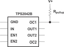
TPS2041B TPS2042B TPS2043B TPS2044B  TPS2051B TPS2052B TPS2053B TPS2054B Typical Circuit for the 
OC Pin (Example, TPS2042B)Figure 9-2 Typical Circuit for the OC Pin (Example, TPS2042B)