JAJU648A November   2018  – April 2022 TLV3601 , TLV3601-Q1 , TLV3603 , TLV3603-Q1


  1.   概要
  2.   Resources
  3.   特長
  4.   アプリケーション
  5.   5
  6. 1System Description
    1. 1.1 Key System Specifications
  7. 2System Overview
    1. 2.1 Block Diagram
    2. 2.2 Design Considerations
      1. 2.2.1 Amplifier and Comparator
      2. 2.2.2 Digital Processing and Control
      3. 2.2.3 Optical Components
        1. 2.2.3.1 Laser Driver and Laser Diode
        2. 2.2.3.2 Photodiode
      4. 2.2.4 Power Supply
    3. 2.3 Highlighted Products
      1. 2.3.1 OPA858 Operational Amplifier
      2. 2.3.2 TLV3501 and TLV3601/3 High-Speed Comparators
      3. 2.3.3 TDC7201 Time-to-Digital Converter
    4. 2.4 System Design Theory
      1. 2.4.1 Transimpedance Amplifier
        1. 2.4.1.1 Bandwidth
        2. 2.4.1.2 Stability Considerations
        3. 2.4.1.3 Noise Performance
      2. 2.4.2 Time-of-Flight Measurement
      3. 2.4.3 Simulations
        1. 2.4.3.1 Bandwidth Simulation
        2. 2.4.3.2 Noise Simulation
        3. 2.4.3.3 OPA858 Loop-Gain and Phase Margin Simulation
  8. 3Hardware, Software, Testing Requirements, and Test Results
    1. 3.1 Required Hardware and Software
      1. 3.1.1 Hardware
      2. 3.1.2 Software
    2. 3.2 Testing and Results
      1. 3.2.1 Test Setup
        1. 3.2.1.1 Getting Started: System Setup
          1. 3.2.1.1.1 Laser-Driver Setup
          2. 3.2.1.1.2 Receiver and Optical Setup
      2. 3.2.2 Test Results
        1. 3.2.2.1 Verification and Measured Performance
          1. 3.2.2.1.1 Pulse Response Measurements
            1. 3.2.2.1.1.1 Pulse Response Settling
            2. 3.2.2.1.1.2 Pulse Response vs Output Pulse Width
            3. 3.2.2.1.1.3 Rise and Fall Time
            4. 3.2.2.1.1.4 Overdriven Response
          2. 3.2.2.1.2 Time-of-Flight Test
          3. 3.2.2.1.3 Time-of-Flight Measurement Error Sources
  9. 4Design Files
    1. 4.1 Schematics
    2. 4.2 Bill of Materials
    3. 4.3 PCB Layout Recommendations
      1. 4.3.1 Layout Prints
    4. 4.4 Altium Project
    5. 4.5 Gerber Files
  10. 5Related Documentation
    1. 5.1 Trademarks
  11. 6About the Author
  12. 7Revision History

Bandwidth Simulation

Figure 2-7 shows the TINA-TI™ simulation schematic for the OPA858 amplifier design. The current source represents the photodiode and the 1.1-pF capacitor is the equivalent capacitance from the NR-7500 photodiode. The noninverting input of the amplifier is biased positive because the input of the photodiode only pulses one direction.
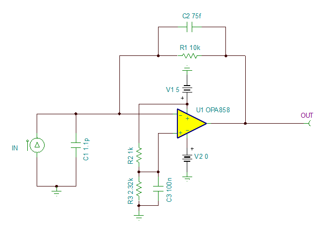
GUID-6EC43AFB-B374-442A-BE59-FDC96EAC694B-low.gifFigure 2-7 OPA858 Bandwidth and Noise Simulation Schematic

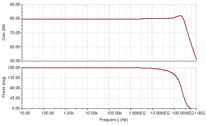
Figure 2-8 shows the bandwidth simulation results of the OPA858 transimpedance circuit. The simulated bandwidth is higher than the predicted value in Section 2.4.1.1. This difference in value is because the model more accurately models the open-loop response of the amplifier and the calculated value is only based on a first-order approximation of the circuit.
GUID-5BEE91B5-2A36-4CB9-A3A3-C5860C1119BC-low.gifFigure 2-8 OPA858 Bandwidth Simulation Results