JAJU648A November   2018  – April 2022 TLV3601 , TLV3601-Q1 , TLV3603 , TLV3603-Q1


  1.   概要
  2.   Resources
  3.   特長
  4.   アプリケーション
  5.   5
  6. 1System Description
    1. 1.1 Key System Specifications
  7. 2System Overview
    1. 2.1 Block Diagram
    2. 2.2 Design Considerations
      1. 2.2.1 Amplifier and Comparator
      2. 2.2.2 Digital Processing and Control
      3. 2.2.3 Optical Components
        1. 2.2.3.1 Laser Driver and Laser Diode
        2. 2.2.3.2 Photodiode
      4. 2.2.4 Power Supply
    3. 2.3 Highlighted Products
      1. 2.3.1 OPA858 Operational Amplifier
      2. 2.3.2 TLV3501 and TLV3601/3 High-Speed Comparators
      3. 2.3.3 TDC7201 Time-to-Digital Converter
    4. 2.4 System Design Theory
      1. 2.4.1 Transimpedance Amplifier
        1. 2.4.1.1 Bandwidth
        2. 2.4.1.2 Stability Considerations
        3. 2.4.1.3 Noise Performance
      2. 2.4.2 Time-of-Flight Measurement
      3. 2.4.3 Simulations
        1. 2.4.3.1 Bandwidth Simulation
        2. 2.4.3.2 Noise Simulation
        3. 2.4.3.3 OPA858 Loop-Gain and Phase Margin Simulation
  8. 3Hardware, Software, Testing Requirements, and Test Results
    1. 3.1 Required Hardware and Software
      1. 3.1.1 Hardware
      2. 3.1.2 Software
    2. 3.2 Testing and Results
      1. 3.2.1 Test Setup
        1. 3.2.1.1 Getting Started: System Setup
          1. 3.2.1.1.1 Laser-Driver Setup
          2. 3.2.1.1.2 Receiver and Optical Setup
      2. 3.2.2 Test Results
        1. 3.2.2.1 Verification and Measured Performance
          1. 3.2.2.1.1 Pulse Response Measurements
            1. 3.2.2.1.1.1 Pulse Response Settling
            2. 3.2.2.1.1.2 Pulse Response vs Output Pulse Width
            3. 3.2.2.1.1.3 Rise and Fall Time
            4. 3.2.2.1.1.4 Overdriven Response
          2. 3.2.2.1.2 Time-of-Flight Test
          3. 3.2.2.1.3 Time-of-Flight Measurement Error Sources
  9. 4Design Files
    1. 4.1 Schematics
    2. 4.2 Bill of Materials
    3. 4.3 PCB Layout Recommendations
      1. 4.3.1 Layout Prints
    4. 4.4 Altium Project
    5. 4.5 Gerber Files
  10. 5Related Documentation
    1. 5.1 Trademarks
  11. 6About the Author
  12. 7Revision History
Overdriven Response

Figure 3-7 shows the pulse response of the OPA858 without an optical attenuator in the signal path. In this condition, the amplifier output is saturated and extends the 20-ns input pulse to a measured pulse width of 36 ns and increases the fall time to 1.5 ns compared to the non-saturated graph in Figure 3-4. The pulse extension does not affect this design because the measurement is triggered on the falling edge, but the fall time can potentially add an error as discussed further in Section 3.2.2.1.2. The plot in Figure 3-7 also shows the maximum achievable signal swing of 2.6 V when measured from the bias set in the design.
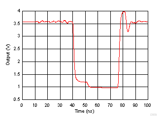
GUID-F802827A-76A2-4CA0-B26E-60DD3BB2BE8C-low.gifFigure 3-7 OPA858 Overdriven Response