SBOA367B December 2019 – June 2022 TLV9001 , TLV9002 , TLV9004 , TLV9051 , TLV9052 , TLV9054 , TLV9061 , TLV9062 , TLV9064
- Designing for TLV90xxS operational amplifiers with shutdown
- Trademarks
- 1 Introduction
- 2 Shutdown Specifications
- 3 SHDN Pin Limits and Connections
- 4 Output Behavior During Enable and Shutdown
- 5 Enable Time and Shutdown Time Factors
- 6 Impact on Commonly Used Circuit Configurations
- 7 Advanced Circuit Functionality Using Amplifiers With Shutdown
- 8 Conclusion
- 9 References
- 10Revision History
5.4 Feedback Path
A similar analysis can be done to determine the effects of closed-loop impedance and gain on shutdown times. Consider three different types of closed-loop configurations:
- Unity gain buffer
- Non-inverting amplifier with a gain of 11 and feedback resistors of 18 kΩ (Rf) and 1.8 kΩ (Ri)
- Non-inverting amplifier with a gain of 11 and feedback resistors of 180 kΩ (Rf) and 18 kΩ (Ri)
An example circuit for the non-inverting configuration is shown in Figure 5-3. Again, the left portion of the image shows the configuration during enabled operation while the right portion shows the effective circuit when the amplifier is in shutdown mode.
 Figure 5-3 Non-Inverting Amplifier Circuit
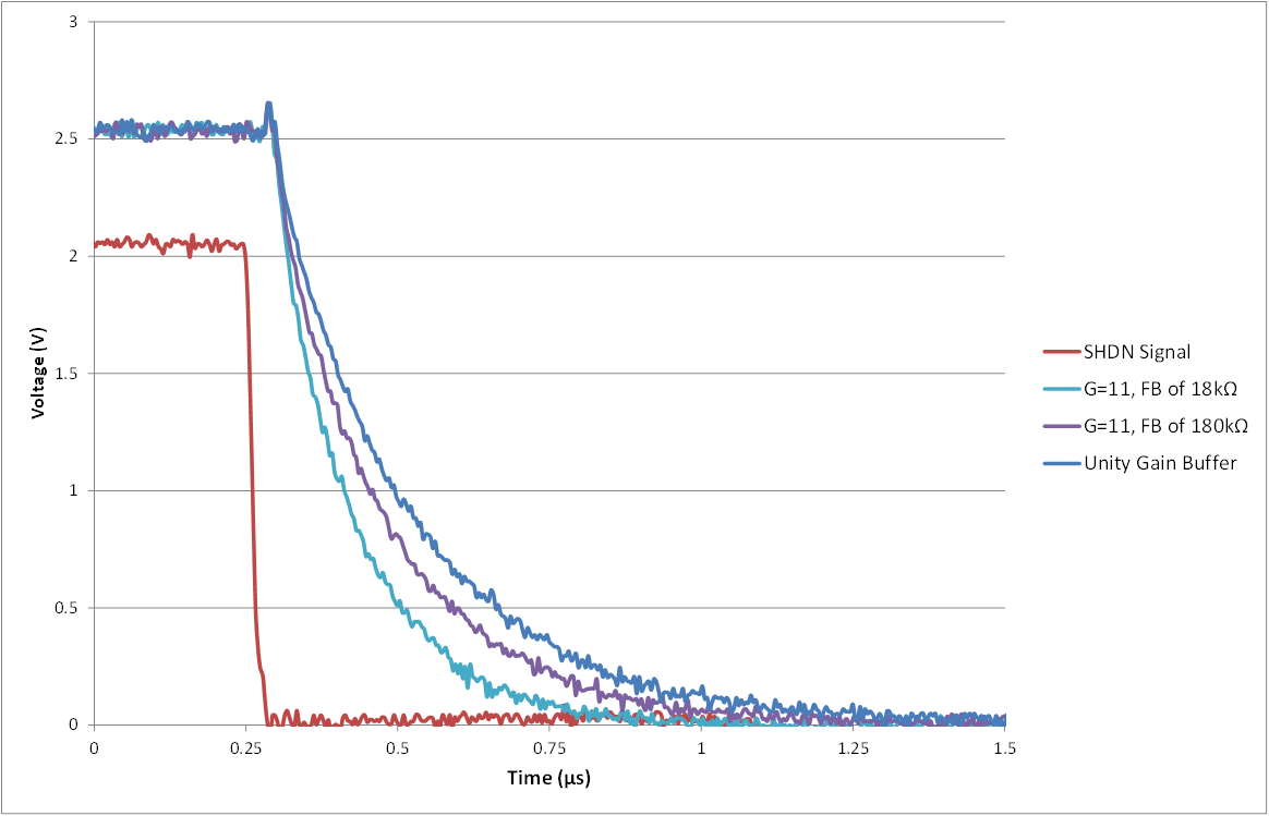
Notice that when the amplifier is turned off, the feedback resistors, Rf and Ri, offer a resistive pulldown path to ground for the output. Similar to the case of the purely resistive load, this alternative path to ground can shorten shutdown times. However, the key here is that the shutdown time is heavily influenced by the total resistance in the feedback network and not by the gain set by the resistor ratio. In other words, the closed loop gain is not the dominant factor. The reason for this, as in the case of the output load examples, is that excessively large feedback resistors will form significant RC combinations with parasitic capacitances and lead to longer shutdown times.
Figure 5-4 displays the shutdown behavior of the TLV906xS for a unity gain buffer and gain of 11 V/V using two different feedback resistances. The measurements were taken on channel 1 while channel 2 remained on at all times.
 Figure 5-4 Closed-Loop Configuration and Shutdown TLV9062S