SCDA046A January 2024 – July 2024 TMUX7308F , TMUX7309F , TMUX7348F , TMUX7349F , TMUX7411F , TMUX7412F , TMUX7413F , TMUX7436F , TMUX7462F
3 System Level Lab Test Procedure and Results of EFT Burst Testing
In this lab experiment a 5kHz, 5% duty cycle signal was sent onto the line as a simulated EFT burst. Due to lab waveform generator limitations, this test only looks at protection from voltages that are produced after the clamping of a TVS diode on the signal line. While no TVS diode was used during this experiment, note that any clamped voltage within the fault protected multiplexer's acceptable input range (± 60V) is blocked by the devices OVP feature and provide protection from EFT burst. Other limitations include, passive components being chosen based on availability during testing and the ac cap replacing capacitive coupling that happens when a burst pulse is sent onto the shield of a wire in a PLC communication system.
 Figure 3-1 EFT Burst Test Setup
Figure 3-1 shows the setup for this EFT burst test using a XTR300 amplifier in Vout mode sending 10v down the analog signal line. First, the RC load provides stability to the amplifier and maintains the 10V signal on the line during the switching of the mux. The RC load represents part of an analog output module.
The switch can recover faster than the time between EFT burst pulses which stops the link from discharging. If this device's fault recovery time was longer than the time between pulses, then the switch stays open circuit and never reconnect the signal line leading to the loss of voltage on the signal link line. This causes failure in communication between the analog input and output modules.
Typical PLC system RC loads range from 1nf-10nf and 100kΩ - 1MΩ. As a result, we can see that systems RC time constants range from 100us to 10,000us. These time constants represent how much time the signal link takes to discharge. This means the switch can recover faster and recharge the signal before the signal can discharge on the line, leading to a consistent 10v signal link that sees little to no degradation during EFT burst.
The next part of the analog output module is the low pass filter which serves the purpose of protecting/smoothing out the EFT burst signal before reaching the ADC input. This low pass filter is another important part of the PLC protection scheme and can be designed directly or can be found integrated inside some ADCs. The expected behavior is that the link is not interrupted and the values on the line are allowed to change within specified ranges provided by the system designers. Figure 3-2 shows the EFT burst test setup with probe locations. This is important so we can understand the behavior of the system with TI’s fault protected multiplexers.
 Figure 3-2 EFT Burst Test Setup With Probe
Locations
Figure 3-2 EFT Burst Test Setup With Probe
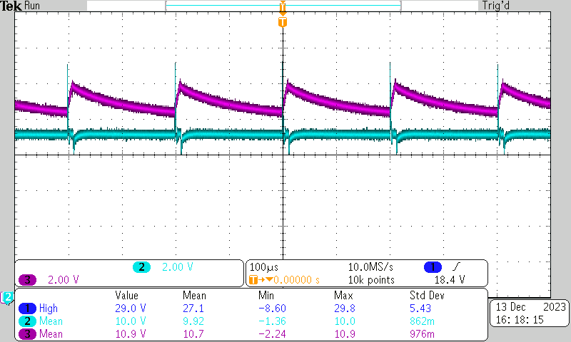
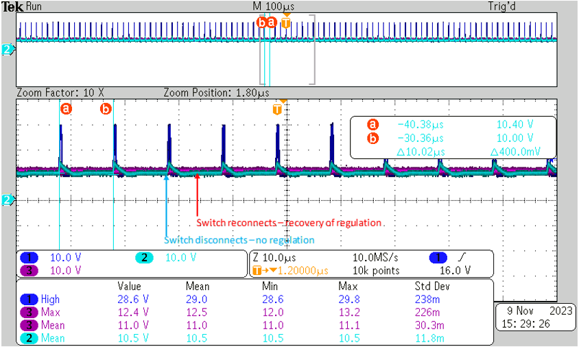
LocationsThe following images show waveforms for the EFT burst test. Looking at the TMUX7462F images (Figure 3-3 and Figure 3-4) show that the fault protected multiplexer is operating as intended and reconnecting the signal line quickly between burst pulses leading to a continuous 10V signal being sent from the drain pin of the mux to the low pass filter. The difference between the light blue and purple line is called the offset voltage and is a result of the EFT burst being smoothed out by the low pass filter.
 Figure 3-3 5kHz Simulated EFT Burst Test TMUX7462F Zoomed
In
 Figure 3-4 TMUX7462F Zoomed Out
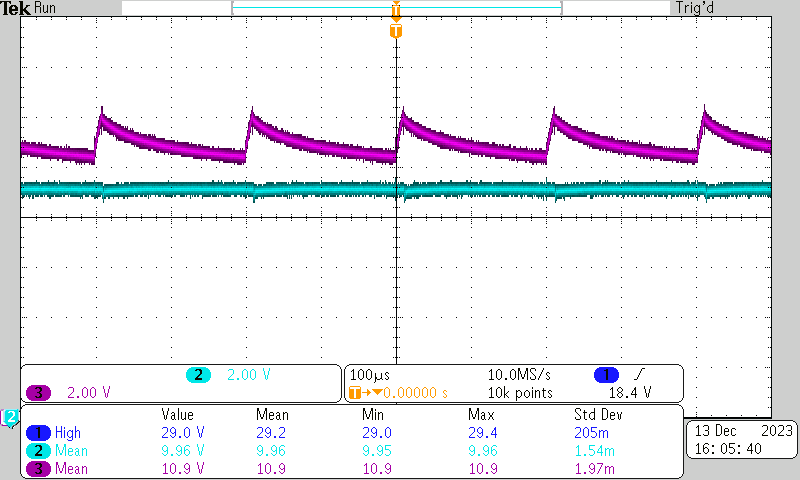
When looking at the TMUX7309F (Figure 3-5 and Figure 3-6) show how the system behaves as expected and reconnects the signal link quickly between burst pulses leading to a continuous uninterrupted communication. The offset voltage error during the TMUX7309F test is similar to the TMUX7462F test. Note that when the EFT burst testing is done, both devices pass the amplifier signal from drain to source with no interruption.
 Figure 3-5 5kHz Simulated EFT Burst Test TMUX7309F Zoomed
In
 Figure 3-6 TMUX7309F Zoomed Out
Table 3-1 shows more information on the offset voltage for both system setups.
| TMUX7309F | TMUX7462F | |
|---|---|---|
| Burst Test Offset Measurements( 5kHz) | 0.94V | 0.9V |
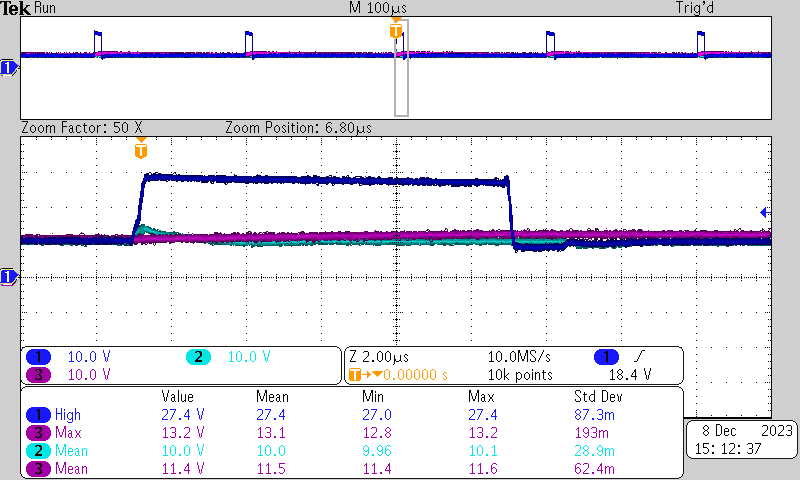
In addition, Figure 3-7 shows a 100kHz simulated EFT burst test being performed on the TMUX7462F. Note that this test has the same setup and probe locations as the previous 5kHz test. Due to both tests having the same duty cycles, the error is very similar. This zoomed in picture shows when the switch reconnects and brings the link back to regulation after about 5us.
 Figure 3-7 100kHz Simulated EFT Burst Test TMUX7462F
Finally, the offset voltage (the difference between the light blue and purple line) comes from the EFT burst signal injecting energy on the line that shows as an added DC value even after the low pass filter. The expected offset voltage is based on the duty cycle of the EFT burst signal put onto the signal lines.
To understand why there is offset voltage and how that voltage is smaller with a standard EFT burst profile, we can look at the following example. If we send a 0 to 18v and 5% duty cycle signal onto the 10V signal line to simulate an EFT burst, we see approximately 0.9V (18*0.05) added onto the line and show up as an error on the analog output or output of low pass filter. To see what the injected voltage is going to be on the line during an EFT burst test with a standard burst profile, please follow the method below.
- First, find the duty cycle of the EFT Burst
signals (Figure 1-2 and Figure 1-3).
- Time between pulses (TP) = 10us for 100kHz EFT burst or 200us for 5kHz EFT burst test and Pulse Duration (tp)= 50ns
- Next, find the duty cycle of the EFT Burst
signals when sent in the burst packets as outlined in (Figure 1-3) Test Repetition Times.
- Duty cycle of EFT Burst = 50ns/10us = 0.5% and Burst Packet Duty cycle = 0.75ms/300ms = 0.25% (100kHz test)
- Duty cycle of EFT Burst = 50ns/200us = 0.025% and Burst Packet Duty cycle = 15ms/300ms = 5% (5kHz test)
- Finally, multiply the different duty cycles to
see what error can be introduced with a standard EFT Burst profile.
- Duty Cycles of standard EFT Burst signal
- 100kHz test = 0.5% * 0.25% = 0.00125%
- 5kHz test = 0.025% * 5% = 0.00125%
So, a system designer can expect to see (18 x 0.00125% = 0.000225 volts) or 0.225mV added on the 10V signal line if 18V is the peak voltage of EFT burst signal. If we compare that error to what is typically acceptable for customer designs, which is 1-2%, then we can see that 0.225mV provides even better performance than the customer allowable error of 100-200mv.
Note that the fault protected multiplexers do not introduce the offset error themselves and PLC communication systems in this report falls into Performance Criteria A Performance within specification limits as the added EFT Burst signal error is acceptable for the customer application.