SLAAED3A October 2023 – May 2024 TAA5212 , TAA5242 , TAC5111 , TAC5112 , TAC5142 , TAC5211 , TAC5212 , TAC5242
1 Introduction
TAC5212 is a CODEC with dual-channel analog-to-digital converters whose input pins (IN1P/M and IN2P/M) are configurable as differential inputs, single-ended inputs or single-ended mux inputs in AC or DC coupling. The type of input is configured through ADC_CH1_INSRC, the input impedance is configured through ADC_CH1_IMP and the coupling and common-mode tolerance is configured through ADC_CH1_CM_TOL.
| Input Configuration Setting | B0_P0_R80 (ADC_CH1_CFG0) [7:6] | Input Channel Configuration |
|---|---|---|
| 0 | ADC_CH1_INSRC=[00] | Analog differential input |
| 1 | ADC_CH1_INSRC=[01] | Analog single-ended input |
| 2 | ADC_CH1_INSRC=[10] | Analog single-ended mux INP1 input |
3 | ADC_CH1_INSRC=[11] | Analog single-ended mux INM1 input |
| Input Impedance Setting | B0_P0_R80 (ADC_CH1_CFG0) [5:4] | ADC Channel 1 Input Impedance |
|---|---|---|
| 0 | ADC_CH1_IMP=[00] | Typical 5-kΩ input impedance (For 4 Vrms case, is 10-kΩ) |
| 1 | ADC_CH1_IMP=[01] | Typical 10-kΩ input impedance |
| 2 | ADC_CH1_IMP=[10] | Typical 40-kΩ input impedance |
| 3 | ADC_CH1_IMP=[11] | Reserved |
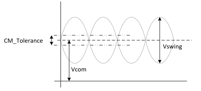
The common-mode tolerance is defined as the variation of the common mode signal of the differential amplifier, this is depicted in Figure 1-1.
 Figure 1-1 Common-Mode Tolerance
In AC-Coupling mode, this device family supports three common mode tolerances; differentially 100 mVpp, 1 Vpp and rail-to-rail (supply to ground) and in DC-Coupling mode, it supports differentially of 1 Vpp and rail-to-rail (supply to ground). This common mode tolerance needs to be selected based on the maximum expected common-mode variation. Since wider common-mode tolerance does degrade other performance parameters, the recommendation is to select the lowest tolerance mode possible.
| Common-Mode Tolerance Setting | B0_P0_R80 (ADC_CH1_CFG0) [3:2] | Input Channel Common-Mode Tolerance |
|---|---|---|
| 0 | ADC_CH1_CM_TOL=[00] | AC-coupled input with common mode variance tolerance supported 50 mVpp for single ended and 100 mVpp for differential configuration |
| 1 | ADC_CH1_CM_TOL=[01] | AC-coupled / DC-coupled input with common mode variance tolerance supported 500 mVpp for single ended and 1 Vpp for differential configuration (Expected SNR degradation of 1-2 dB) |
| 2 | ADC_CH1_CM_TOL=[10] | AC-coupled / DC-coupled input with common mode variance tolerance supported rail to rail (supply to ground) (Expected SNR degradation of approximately 35 dB, High CMRR supported only in this case) |
| 3 | ADC_CH1_CM_TOL=[11] | Reserved |
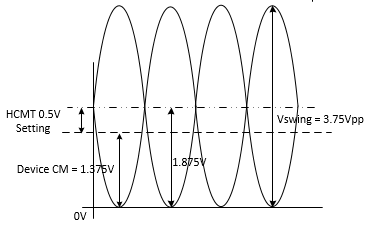
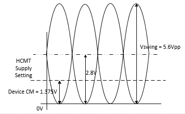
Note that it is important to keep in mind the full-scale range (Vswing) of the device in all modes. This is especially important for large common-mode signals as they will limit the effective input range. In Mode 1 DC-Couple for example, a 500 mVp common voltage variant from the device internal common mode voltage of 1.375 V will limit the Vswing to 3.75 Vpp single-ended or 7.5 Vpp (2.65 Vrms) differential. In mode 2, it can support a common-mode range of 0V to Supply, but there would be no room left for a differential signal to be applied to the input pins at either of these extremes.
 Figure 1-2 Mode 1 Common-Mode Example
 Figure 1-3 Mode 2 Common-Mode Example