SLVAFI4 july 2023 LP5890 , LP5891 , TLC6983 , TLC6984
2.2 Design Scan Line Number
Figure 2-1 shows the DS-PWM algorithm with 32 lines integrated into the TLC6983.The relational expression between frame rate (fframe_rate), segment length (NGCLK_seg), GCLK frequency (fGCLK), line switch time (TSW), scan line number (Nscan_line), sub-period (or says sub-frame) number (Nsub_period), and the blank time (Tblank) in one frame is as following.
 Figure 2-1 DS-PWM Algorithm With 32 Scan
Lines
Figure 2-1 DS-PWM Algorithm With 32 Scan
LinesThe maximum GCLK frequency (fGCLK) allowed is 160 MHz. The minimum allowed line switch time TSW can be set to 45 GCLK. However, at least 1μs to 1.5μs line switch time is recommended. The blank time (Tblank) is equal to 0 in ideal configurations. So, the maximum scan line number allowed is:
Using Equation 4, the calculated result is 19, which is much less than the 32 scans discussed in Section 1 that can be supported by the dual TLC6983 in stackable mode. This result implies that the actual maximum available scan line number is limited to the maximum PWM resolution required by the product and the maximum GCLK frequency generated by the driver itself. Restated, achieing a very high PWM resolution and high scan line number at the same time is very difficult with a limited GCLK frequency. There is a tradeoff between the PWM resolution and scan line number. The higher the integration density (with high scan line number), the lower the PWM resolution. For instance, consider the effect of reducing resolution from 16 bits to 15 bits. The PWM resolution cannot be lowered because display effect is then lowered, instead, scan line number must be reduced. This tradeoff is one of the reasons why a products on the market can have a driver that can support 16 or higher bits but the “real” 16-bit PWM resolution is much lower. This relationship is also why some high-end products on the market have very small scan line numbers, to acquire excellent display effects (from 16-bits, 20-bits or higher PWM resolution).
Returning back to the design requirements, the LED panel module (96 × 108) has 96 columns; dual TLC6983 in stackable mode (sub-block) can support 32 × 32 RGB pixels (32 RGB channels and 32 scans). So, all RGB channels can be fully utilized (96 / 32 = 3 sub-blocks in row). A cascade device number (Ncascade) of 6 is recommended for this use case (96 / 16 = 6). The cascade number can be set higher, such as 12 devices in cascade, but more cascade devices need higher SCLK frequency (SCLK design is discussed in later sections) which can cause worse EMI, and also places more requirements on the FPGA of the controller.
For scan lines, the following relationship is considered: ROUNDUP(108 / 19, 0) = 6, 108 / 6 = 18. This calculation results in 6 sub-blocks in column. 108 is divisible by 18 and the scan line number (Nscan_line) can be set to 18. If the numerator is not divisible,then spacing out the scan lines as far as possible for loading sharing purpose is recommended. For example, if the maximum allowed scan line number is 16, that scan line suggests that 3 sub-blocks have 16 scan lines and 4 sub-blocks have 15 scan lines in a column.
The equation for the minimum GCLK frequency is:
Using the preceding figures, the result of the calculation with this equation 147.8 MHz.
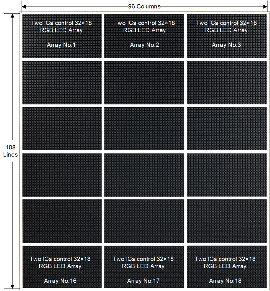
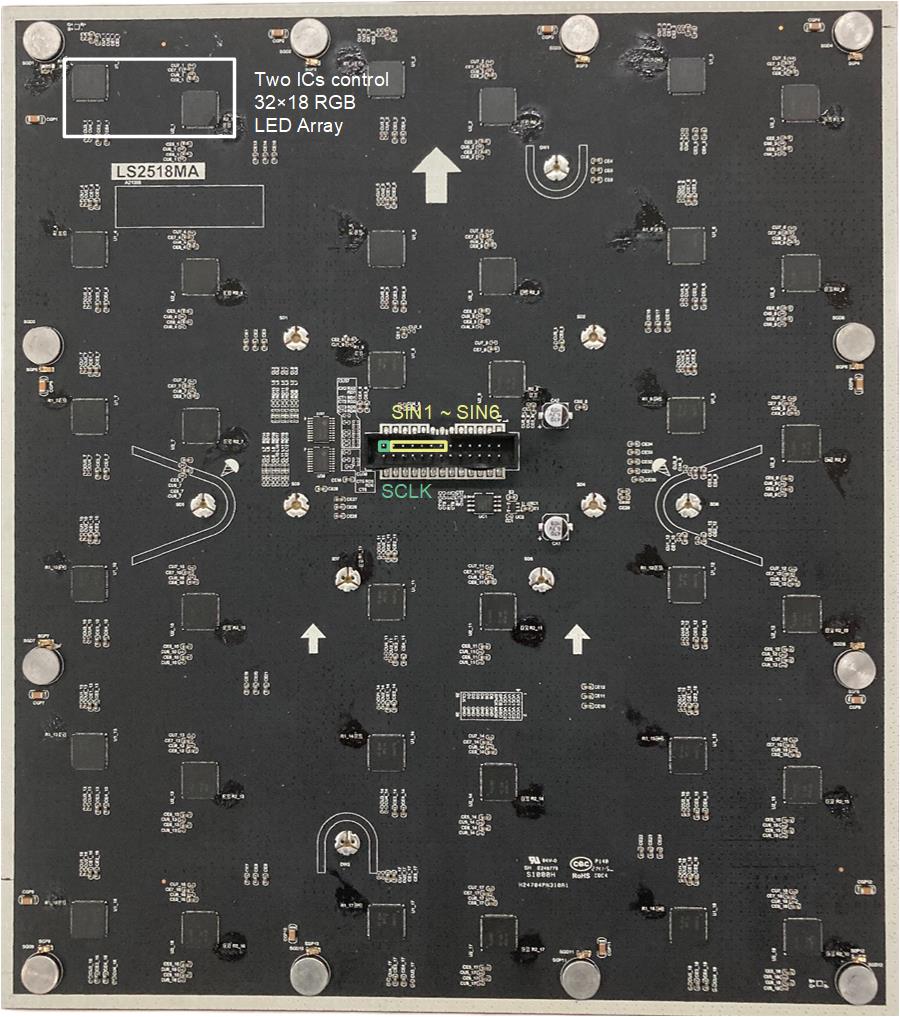
Figure 2-2 shows more details of the LED panel (96x108) highlighted in Figure 1-1. The LED panel module is decomposed into eighteen 32 × 18 sub-blocks (6 groups in row). Each sub-block has the dual TLC6983 in stackable mode connection. Figure 2-3 and Figure 2-4 show the physical prototype board.
 Figure 2-2 Details of the LED Panel
Module (96 × 108)
 Figure 2-3 The Front of the LED Panel
Module Prototype Board (96 × 108)
 Figure 2-4 The Back of the LED Panel
Module Prototype Board (96 × 108)