SNAA386 November 2023 CDCE6214 , CDCE6214-Q1 , CDCE6214Q1TM , LMK00301 , LMK00304 , LMK00306 , LMK00308 , LMK00334 , LMK00334-Q1 , LMK00338 , LMK03318 , LMK03328 , LMK3H0102 , LMK6C , LMK6H , LMKDB1104 , LMKDB1108 , LMKDB1120 , LMKDB1202 , LMKDB1204
5.1.5 Time Domain PCIe Measurement Result
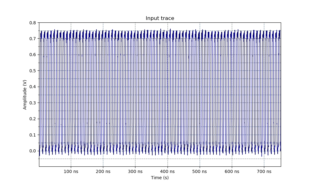
Figure 5-6 is the time domain capture of the OUT0_P and OUT0_N outputs of the LMK3H0102 as measured by the oscilloscope for the non-SSC case. These results are exported to text files, which can be read by the Texas Instruments PCIe Reference Clock Analysis Tool and analyzed for compliance.
 Figure 5-4 LMK3H0102 PCIe Time Domain
Capture
Figure 5-4 LMK3H0102 PCIe Time Domain
CaptureTable 5-6 shows the result of the oscilloscope measurement after analysis. For the LMK3H0102, all of the parameters meet the limits specified in Table 4-2.
| Parameter | Units | Minimum | Average | Maximum | Limit | Status |
|---|---|---|---|---|---|---|
| VCross | mV | 396.62 | 407.61 | 416.73 | 250 mV to 550 mV | Pass |
| VHigh | mV | 720.0 | 720.0 | 150 mV | Pass | |
| VLow | mV | –12.0 | –12.0 | –150 mV | Pass | |
| VRingback | mV | 621.9476 | 645.43 | 100 mV | Pass | |
| Period | ns | 9.9 | 9.996 | 10.1 | 9.847 ns to 10.203 ns | Pass |
| Duty Cycle | % | 50.02 | 50.58 | 51.021 | 40% to 60% | Pass |
| VOvershoot | mV | 28.26 | 40.0 | 300 mV | Pass | |
| VUndershoot | mV | –32.28 | –48.0 | –300 mV | Pass | |
| Rising Edge Rate | V/ns | 2.24 | 2.584 | 2.92 | 0.6 V/ns to 4.0 V/ns | Pass |
| Falling Edge Rate | V/ns | 2.12 | 2.612 | 3.08 | 0.6 V/ns to 4.0 V/ns | Pass |