SNVA559C September 2012 – February 2019 LM2574 , LM2575-N , LM2575HV , LM2576 , LM2576HV , LM2577
-
Switching regulator fundamentals
- Trademarks
- 1 Switching Fundamentals
- 2 Switching Converter Topologies
- 3 Application Hints for Switching Regulators
- 4 Application Circuits
- 5 References and Related Products
- Revision History
2.10 Full-Bridge Converter
The Full-Bridge converter requires a total of four switching transistors to perform DC/DC conversion. The full bridge is most often seen in applications that are powered directly from the AC line, providing load power of 1 kW to 3 kW.
Operating offline, the full bridge converter typically uses about 300 V of unregulated DC voltage for power conversion (the voltage that is obtained when a standard 230 VAC line is rectified and filtered).
An important feature of this design is the isolation from the AC line provided by the switching transformer. The PWM control circuitry is referenced to the the output ground, requiring a dedicated voltage rail (usually powered from a small 60-Hz transformer) to run the control circuits.
The base drive voltages for the switch transistors (which are provided by the PWM chip) have to be transformer-coupled because of the required isolation.
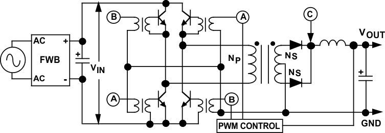
Figure 15 shows a simplified schematic diagram of a Full-Bridge converter.
 Figure 15. Full-Bridge Converter
 The transformer primary is driven by the full voltage VIN when either of the transistor sets (A set or B set) turns on. The full input voltage utilization means the Full-Bridge can produce the most load power of all the converter types. The timing diagram is identical to the Half-Bridge, as shown in Figure 14.
Primary and secondary current flows in the transformer during the switch on times, while the output capacitor discharges into the load when both transistors are off.
Equation 6 is the equation for the output voltage (see Figure 14):
The peak voltage of the transformer secondary pulses (VPK) is given by Equation 7: