SNVU628 February   2020 LM5155 , LM5155-Q1 , LM51551 , LM51551-Q1


  1.   LM5155EVM-SEPIC User's Guide
    1.     Trademarks
    2. 1 Features and Electrical Performance
      1. 1.1 Electrical Parameters
      2. 1.2 EVM Power Derating Curve
      3. 1.3 Terminals and Signal Test Points
    3. 2 Application Schematic
    4. 3 EVM Picture
    5. 4 Test Setup and Procedure
      1. 4.1 Bench Setup
      2. 4.2 Test Equipment
      3. 4.3 Precautions
    6. 5 Test Data
      1. 5.1 Efficiency
      2. 5.2 Output Regulation
      3. 5.3 Typical Power Up
      4. 5.4 Output Ripple Voltage
      5. 5.5 Coupled Inductor Currents
      6. 5.6 Dynamic DIR Change
      7. 5.7 Step Load Response
      8. 5.8 Bode Plots
      9. 5.9 Overloading Hiccup Mode
    7. 6 Design Files
      1. 6.1 Schematics
      2. 6.2 Bill of Materials
      3. 6.3 Board Layout

Board Layout

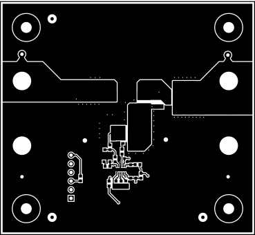
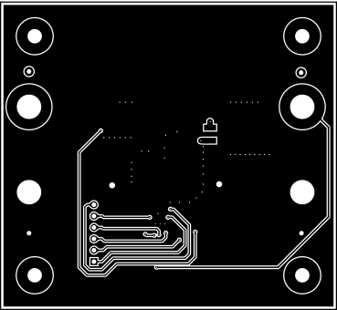
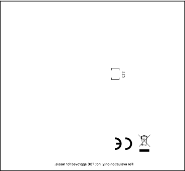
The EVM PC Board consists of two copper layers, and the board includes various headers for flexible configurations suitable for different applications. Figure 20 through Figure 23 show the EVM PCB artwork.

Layer_1_Top_Silk_SNVU628.gifFigure 20. EVM Top Layer Silkscreen
Layer_2_Top_copper_SNVU628.gifFigure 21. EVM Top Layer Copper
Layer_3_Bottom_copper_SNVU628.gifFigure 22. EVM Bottom Layer Copper
Layer_4_Bot_layer_Silk_xray_SNVU628.gifFigure 23. EVM Bottom Layer Silkscreen