SPRACY9 March 2023 F29H850TU , F29H850TU , TMS320F2800132 , TMS320F2800132 , TMS320F2800133 , TMS320F2800133 , TMS320F2800135 , TMS320F2800135 , TMS320F2800137 , TMS320F2800137 , TMS320F2800152-Q1 , TMS320F2800152-Q1 , TMS320F2800153-Q1 , TMS320F2800153-Q1 , TMS320F2800154-Q1 , TMS320F2800154-Q1 , TMS320F2800155 , TMS320F2800155 , TMS320F2800155-Q1 , TMS320F2800155-Q1 , TMS320F2800156-Q1 , TMS320F2800156-Q1 , TMS320F2800157 , TMS320F2800157 , TMS320F2800157-Q1 , TMS320F2800157-Q1 , TMS320F280021 , TMS320F280021 , TMS320F280021-Q1 , TMS320F280021-Q1 , TMS320F280023 , TMS320F280023 , TMS320F280023-Q1 , TMS320F280023-Q1 , TMS320F280023C , TMS320F280023C , TMS320F280025 , TMS320F280025 , TMS320F280025-Q1 , TMS320F280025-Q1 , TMS320F280025C , TMS320F280025C , TMS320F280025C-Q1 , TMS320F280025C-Q1 , TMS320F280033 , TMS320F280033 , TMS320F280034 , TMS320F280034 , TMS320F280034-Q1 , TMS320F280034-Q1 , TMS320F280036-Q1 , TMS320F280036-Q1 , TMS320F280036C-Q1 , TMS320F280036C-Q1 , TMS320F280037 , TMS320F280037 , TMS320F280037-Q1 , TMS320F280037-Q1 , TMS320F280037C , TMS320F280037C , TMS320F280037C-Q1 , TMS320F280037C-Q1 , TMS320F280038-Q1 , TMS320F280038-Q1 , TMS320F280038C-Q1 , TMS320F280038C-Q1 , TMS320F280039 , TMS320F280039 , TMS320F280039-Q1 , TMS320F280039-Q1 , TMS320F280039C , TMS320F280039C , TMS320F280039C-Q1 , TMS320F280039C-Q1 , TMS320F280040-Q1 , TMS320F280040-Q1 , TMS320F280040C-Q1 , TMS320F280040C-Q1 , TMS320F280041 , TMS320F280041 , TMS320F280041-Q1 , TMS320F280041-Q1 , TMS320F280041C , TMS320F280041C , TMS320F280041C-Q1 , TMS320F280041C-Q1 , TMS320F280045 , TMS320F280045 , TMS320F280048-Q1 , TMS320F280048-Q1 , TMS320F280048C-Q1 , TMS320F280048C-Q1 , TMS320F280049 , TMS320F280049 , TMS320F280049-Q1 , TMS320F280049-Q1 , TMS320F280049C , TMS320F280049C , TMS320F280049C-Q1 , TMS320F280049C-Q1 , TMS320F28075 , TMS320F28075 , TMS320F28075-Q1 , TMS320F28075-Q1 , TMS320F28076 , TMS320F28076 , TMS320F28374D , TMS320F28374D , TMS320F28374S , TMS320F28374S , TMS320F28375D , TMS320F28375D , TMS320F28375S , TMS320F28375S , TMS320F28375S-Q1 , TMS320F28375S-Q1 , TMS320F28376D , TMS320F28376D , TMS320F28376S , TMS320F28376S , TMS320F28377D , TMS320F28377D , TMS320F28377D-EP , TMS320F28377D-EP , TMS320F28377D-Q1 , TMS320F28377D-Q1 , TMS320F28377S , TMS320F28377S , TMS320F28377S-Q1 , TMS320F28377S-Q1 , TMS320F28378D , TMS320F28378D , TMS320F28378S , TMS320F28378S , TMS320F28379D , TMS320F28379D , TMS320F28379D-Q1 , TMS320F28379D-Q1 , TMS320F28379S , TMS320F28379S , TMS320F28384D , TMS320F28384D , TMS320F28384D-Q1 , TMS320F28384D-Q1 , TMS320F28384S , TMS320F28384S , TMS320F28384S-Q1 , TMS320F28384S-Q1 , TMS320F28386D , TMS320F28386D , TMS320F28386D-Q1 , TMS320F28386D-Q1 , TMS320F28386S , TMS320F28386S , TMS320F28386S-Q1 , TMS320F28386S-Q1 , TMS320F28388D , TMS320F28388D , TMS320F28388S , TMS320F28388S , TMS320F28P650DH , TMS320F28P650DH , TMS320F28P650DK , TMS320F28P650DK , TMS320F28P650SH , TMS320F28P650SH , TMS320F28P650SK , TMS320F28P650SK , TMS320F28P659DH-Q1 , TMS320F28P659DH-Q1 , TMS320F28P659DK-Q1 , TMS320F28P659DK-Q1 , TMS320F28P659SH-Q1 , TMS320F28P659SH-Q1
- Abstract
- Trademarks
- 1Introduction
- 2Input Settling Design Steps
-
3Example Circuit Design
- 3.1 Select the ADC
- 3.2 Find the Minimum Op-Amp Bandwidth and RC Filter Ranges
- 3.3 Verify the Op-Amp Model
- 3.4 Build the ADC Input Model
- 3.5 Bias Point Analysis to Determine Voa_ss
- 3.6 Transient Analysis to Determine Voa_ss
- 3.7 Perform Initial Transient Analysis
- 3.8 Iterative Approach to Refine RC Filter Values
- 3.9 Perform Final Transient Analysis
- 3.10 Perform Final Transient Analysis
- 3.11 Further Refinement
- 3.12 Further Simulations
- 3.13 Completed Worksheet
- 4Working With Existing Circuits or Additional Constraints
- 5Summary
- 6References
3.7 Perform Initial Transient Analysis
Now that the circuit is setup for simulation, the first step is to run a basic transient analysis to ensure everything is functioning and to check the initial settling. Performing a transient analysis in PSpice for TI requires the creation of a Time Domain (Transient) simulation profile. Once the simulation profile is created, go to PSpice ➔ Run to perform the analysis.
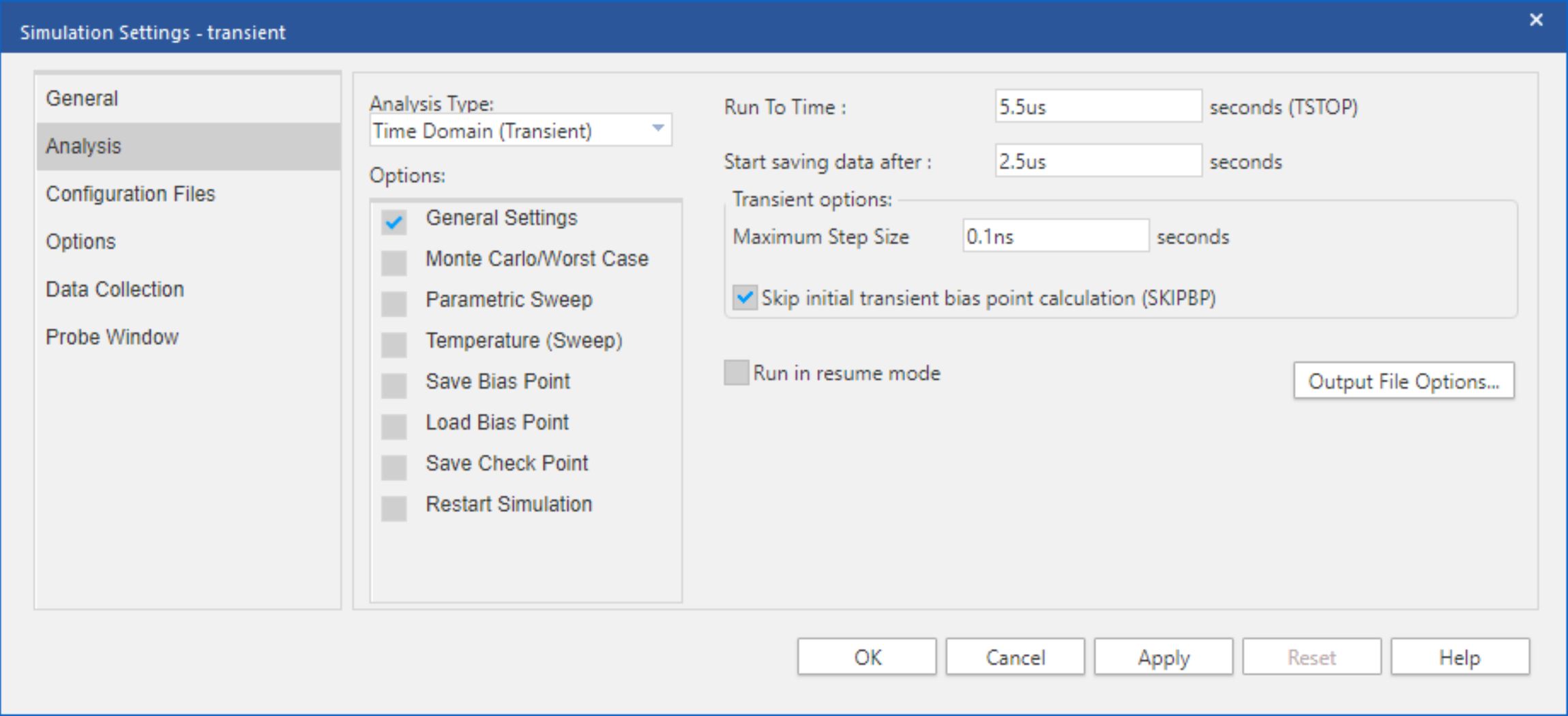
The settling should be captured after allowing the circuit to stabilize for a couple sampling cycles, so a time period of 2.5 μs to 5.5 μs is selected as shown in Figure 3-10. This allows capture of the full 3rd and 4th sampling cycles (each cycle is 1 μs since the trigger frequency is 1 MHz). A maximum step size of 0.1 ns is chosen to produce sufficiently granular simulation results.
 Figure 3-10 F280049 Example Transient
Analysis Simulation Profile
Figure 3-10 F280049 Example Transient
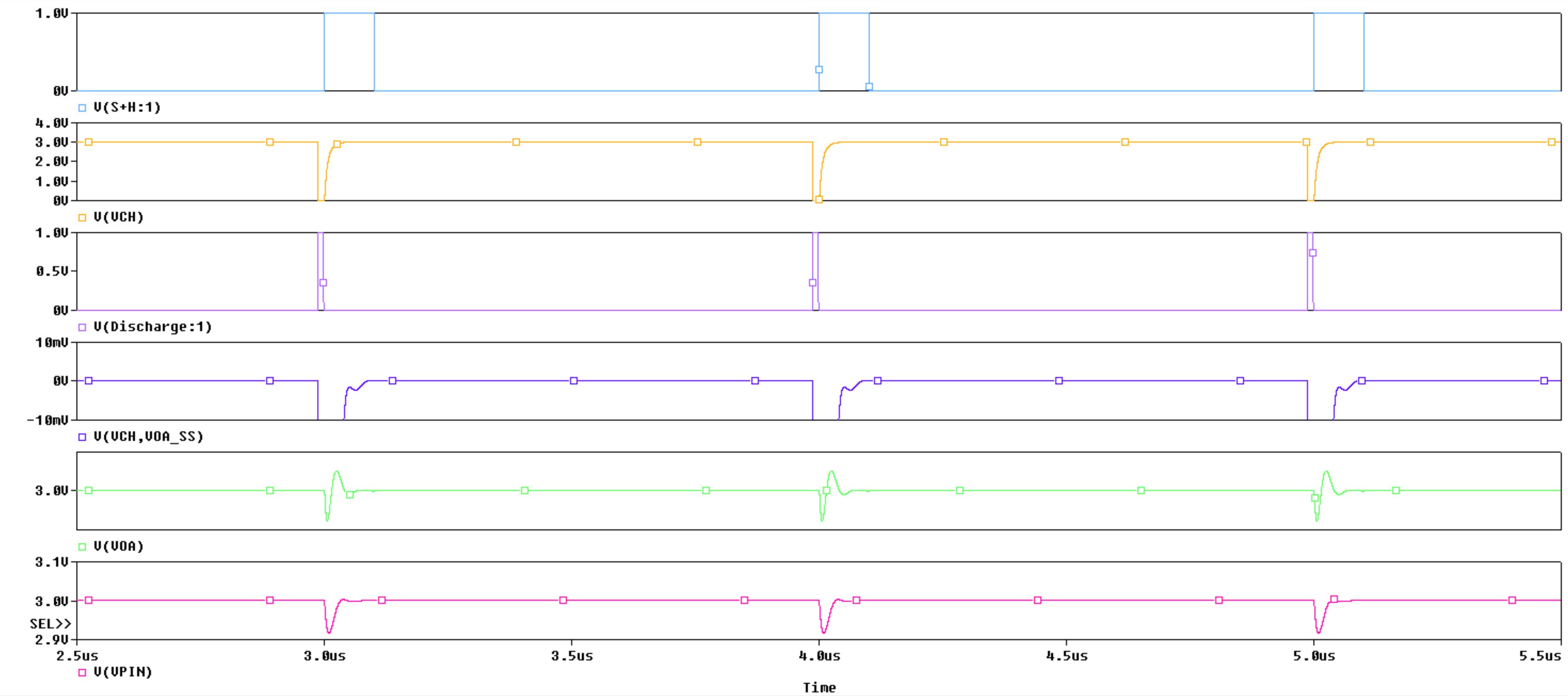
Analysis Simulation ProfileAfter performing the analysis, separate the output waveforms onto different plots. Set Vacq range to 0 V to +1 V. Set Vch range to 0 V to +4 V. Set Vdis range to 0 V to +1 V. Set Verror range to -10 mV to +10 mV. Set Voa range to+2.9 V to +3.1 V. Finally, set Vpin range to+2.9 V to +3.1 V. Alternatively, go to Window ➔ Display Control... using the menu in the upper left of the PSpice for TI simulation window to access a list of preset display configurations provided by TI. Restore the Transient Results display configuration. Note that these preset display configurations are only available in the PSpice for TI projects bundled with this application report. Figure 3-11 shows the output waveforms from the transient simulation. From this output, it is clear that:
- Discharge and acquisition times are functioning as expected
- The transients on Voa and Vpin are of reasonable magnitude (less than 100 mV, so the signal settling will be considered a small signal event)
- Verror is settling to about 69 µV, which is well within the error target of 366 µV
 Figure 3-11 F280049 Example Initial
Transient Results