SPRACZ0A August 2021 – March 2023 F29H850TU , F29H850TU , F29H859TU-Q1 , F29H859TU-Q1 , TMS320F2800132 , TMS320F2800132 , TMS320F2800133 , TMS320F2800133 , TMS320F2800135 , TMS320F2800135 , TMS320F2800137 , TMS320F2800137 , TMS320F2800152-Q1 , TMS320F2800152-Q1 , TMS320F2800153-Q1 , TMS320F2800153-Q1 , TMS320F2800154-Q1 , TMS320F2800154-Q1 , TMS320F2800155 , TMS320F2800155 , TMS320F2800155-Q1 , TMS320F2800155-Q1 , TMS320F2800156-Q1 , TMS320F2800156-Q1 , TMS320F2800157 , TMS320F2800157 , TMS320F2800157-Q1 , TMS320F2800157-Q1 , TMS320F280021 , TMS320F280021 , TMS320F280021-Q1 , TMS320F280021-Q1 , TMS320F280023 , TMS320F280023 , TMS320F280023-Q1 , TMS320F280023-Q1 , TMS320F280023C , TMS320F280023C , TMS320F280025 , TMS320F280025 , TMS320F280025-Q1 , TMS320F280025-Q1 , TMS320F280025C , TMS320F280025C , TMS320F280025C-Q1 , TMS320F280025C-Q1 , TMS320F280033 , TMS320F280033 , TMS320F280034 , TMS320F280034 , TMS320F280034-Q1 , TMS320F280034-Q1 , TMS320F280036-Q1 , TMS320F280036-Q1 , TMS320F280036C-Q1 , TMS320F280036C-Q1 , TMS320F280037 , TMS320F280037 , TMS320F280037-Q1 , TMS320F280037-Q1 , TMS320F280037C , TMS320F280037C , TMS320F280037C-Q1 , TMS320F280037C-Q1 , TMS320F280038-Q1 , TMS320F280038-Q1 , TMS320F280038C-Q1 , TMS320F280038C-Q1 , TMS320F280039 , TMS320F280039 , TMS320F280039-Q1 , TMS320F280039-Q1 , TMS320F280039C , TMS320F280039C , TMS320F280039C-Q1 , TMS320F280039C-Q1 , TMS320F280040-Q1 , TMS320F280040-Q1 , TMS320F280040C-Q1 , TMS320F280040C-Q1 , TMS320F280041 , TMS320F280041 , TMS320F280041-Q1 , TMS320F280041-Q1 , TMS320F280041C , TMS320F280041C , TMS320F280041C-Q1 , TMS320F280041C-Q1 , TMS320F280045 , TMS320F280045 , TMS320F280048-Q1 , TMS320F280048-Q1 , TMS320F280048C-Q1 , TMS320F280048C-Q1 , TMS320F280049 , TMS320F280049 , TMS320F280049-Q1 , TMS320F280049-Q1 , TMS320F280049C , TMS320F280049C , TMS320F280049C-Q1 , TMS320F280049C-Q1 , TMS320F28075 , TMS320F28075 , TMS320F28075-Q1 , TMS320F28075-Q1 , TMS320F28076 , TMS320F28076 , TMS320F28374D , TMS320F28374D , TMS320F28374S , TMS320F28374S , TMS320F28375D , TMS320F28375D , TMS320F28375S , TMS320F28375S , TMS320F28375S-Q1 , TMS320F28375S-Q1 , TMS320F28376D , TMS320F28376D , TMS320F28376S , TMS320F28376S , TMS320F28377D , TMS320F28377D , TMS320F28377D-EP , TMS320F28377D-EP , TMS320F28377D-Q1 , TMS320F28377D-Q1 , TMS320F28377S , TMS320F28377S , TMS320F28377S-Q1 , TMS320F28377S-Q1 , TMS320F28378D , TMS320F28378D , TMS320F28378S , TMS320F28378S , TMS320F28379D , TMS320F28379D , TMS320F28379D-Q1 , TMS320F28379D-Q1 , TMS320F28379S , TMS320F28379S , TMS320F28384D , TMS320F28384D , TMS320F28384D-Q1 , TMS320F28384D-Q1 , TMS320F28384S , TMS320F28384S , TMS320F28384S-Q1 , TMS320F28384S-Q1 , TMS320F28386D , TMS320F28386D , TMS320F28386D-Q1 , TMS320F28386D-Q1 , TMS320F28386S , TMS320F28386S , TMS320F28386S-Q1 , TMS320F28386S-Q1 , TMS320F28388D , TMS320F28388D , TMS320F28388S , TMS320F28388S , TMS320F28P550SJ , TMS320F28P550SJ , TMS320F28P559SJ-Q1 , TMS320F28P559SJ-Q1 , TMS320F28P650DH , TMS320F28P650DH , TMS320F28P650DK , TMS320F28P650DK , TMS320F28P650SH , TMS320F28P650SH , TMS320F28P650SK , TMS320F28P650SK , TMS320F28P659DH-Q1 , TMS320F28P659DH-Q1 , TMS320F28P659DK-Q1 , TMS320F28P659DK-Q1 , TMS320F28P659SH-Q1 , TMS320F28P659SH-Q1
- Abstract
- Trademarks
-
1Introduction
- 1.1
Resources
- 1.1.1 TINA-TI SPICE-Based Analog Simulation Program
- 1.1.2 PSPICE for TI Design and Simulation Tool
- 1.1.3 Application Report: ADC Input Circuit Evaluation for C2000 MCUs
- 1.1.4 TI Precision Labs - SAR ADC Input Driver Design Series
- 1.1.5 Analog Engineer's Calculator
- 1.1.6 TI Precision Labs - Op Amps: Stability Series
- 1.1.7 Related Application Reports
- 1.1.8 Comparison of Schematic Capture and Simulation Tools
- 1.1.9 PSpice for TI ADC Input Models
- 1.1
Resources
-
2Charge-Sharing Concept
- 2.1 Traditional High-Speed ADC Driving Circuits
- 2.2 Increased Cs in High-Speed ADC Driving Circuits
- 2.3 Very Large Cs in ADC Driving Circuits
- 2.4 Charge-Sharing Operation
- 2.5 Sample Rate and Source Impedance vs. Tracking Error
- 2.6 Analytical Solution to Tracking Error
- 2.7 Charge-Sharing in Multiplexed ADCs
- 2.8 Charge-Sharing Circuit Advantages
- 2.9 Charge-Sharing Circuit Disadvantages
- 3Charge Sharing Design Flow
- 4Charge-Sharing Circuit Simulation Methods
- 5Example Circuit Designs
- 6Summary
- A Appendix: ADC Input Settling Motivation
- References
- Revision History
4.5 Measure the Settling Error
Once the circuit is built in PSpice for TI, the steady-state voltage is measured (if applicable), and the sample rate is configured, measuring the settling error is relatively straightforward. This can be accomplished by running a transient analysis over enough periods to ensure that the system reaches steady state. A good starting point is about 30 sampling periods.
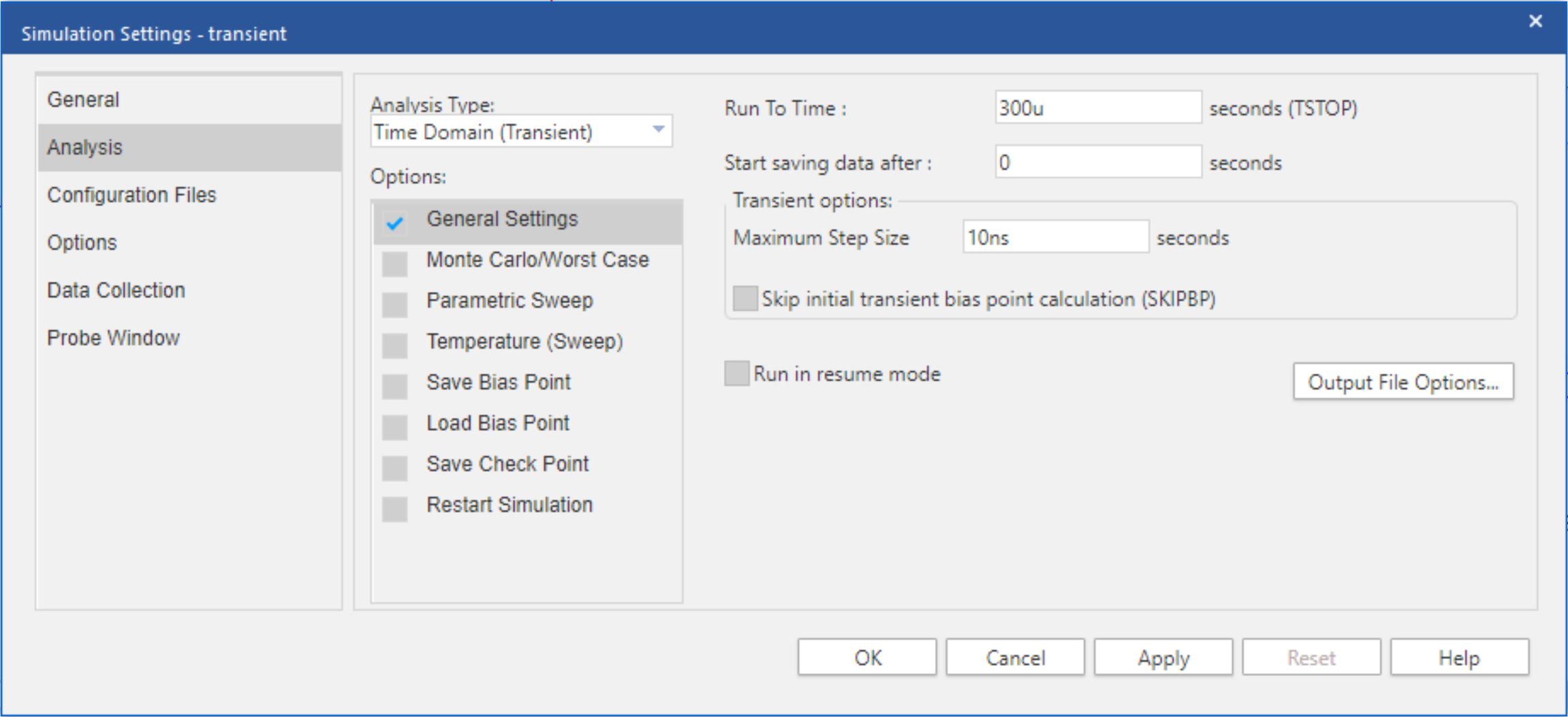
Performing a transient analysis in PSpice for TI requires the creation of a Time Domain (Transient) simulation profile. Once the simulation profile is created, go to PSpice ➔ Run to perform the analysis. An example Time Domain (Transient) simulation profile is shown in Figure 4-12.
 Figure 4-12 Settling Error Simulation
Profile
Figure 4-12 Settling Error Simulation
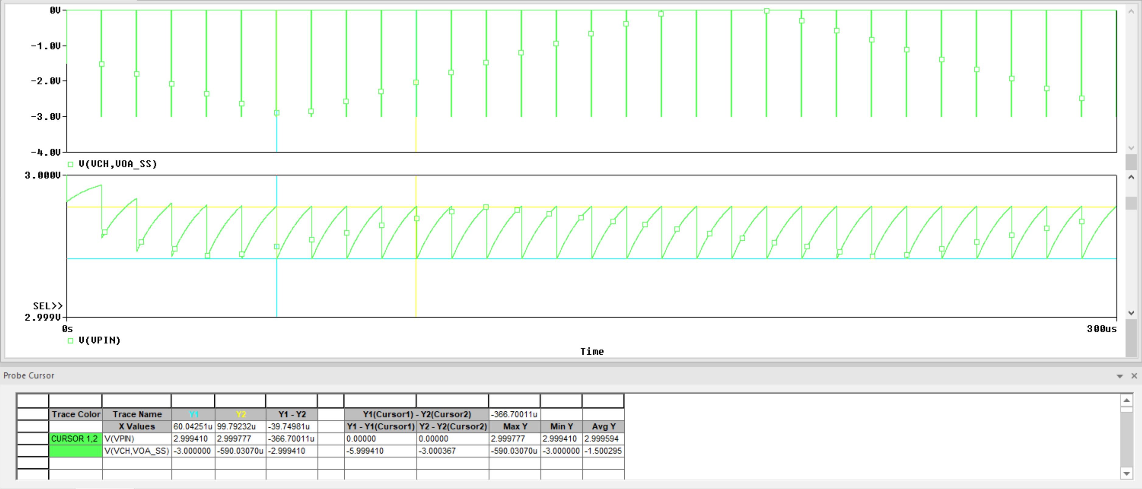
ProfileFigure 4-13 shows the results of this transient simulation profile applied to the example circuit in Figure 4-7 which has 100 nF Cs, 100 Ω Rs , and a 100 kHz sampling rate. After simulation, all outputs other than Verror and Vpin were deleted. The remaining output waveforms were separated onto different plots. Verror range was set to -4 V to 0 V. Vpin range was set to +2.999 V to +3 V. The easiest way to reproduce these display settings is to go to Window ➔ Display Control... using the menu in the upper left of the PSpice for TI simulation window to access a list of preset display configurations provided by TI. Restore the Settling Error display configuration. Note that these preset display configurations are only available in the PSpice for TI projects bundled with this application report.
To measure the total settling error, place a cursor at any point other than the S+H window on the Verror trace. This simulation shows about 590 µV of settling error from this method (yellow cursor). Alternately, the minimum value of Vpin can also be measured. This method shows approximately 3 V - 2.999410 V = 590 µV of settling error (blue cursor).
 Figure 4-13 Settling Error
Measurement
Figure 4-13 Settling Error
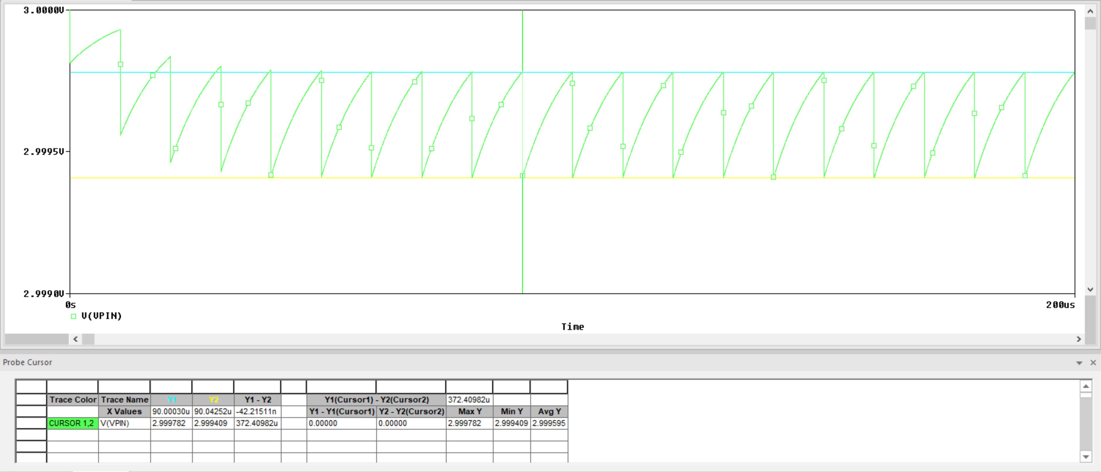
MeasurementIn addition, it is possible to separately measure the charge-share and tracking errors. Figure 4-14 shows the results of narrowing the simulation to 20 periods and also deleting the Verror trace. The distance from 3 V to max value of Vpin in steady state is the approximate tracking error. In this case, the tracking error is 3 V - 2.999782 V = 218 µV (blue cursor). Similarly, the charge-share error is the difference between the tracking error point and the minimum pin voltage in the steady state. In this case, the charge-share error is 2.999782 V - 2.999409 V = 373 µV (blue cursor minus yellow cursor).
 Figure 4-14 Settling Error Component
Measurement