-
TMCS110x Layout Challenges and Best Practices SBOA518 January 2022 TMCS1100 , TMCS1100-Q1 , TMCS1101 , TMCS1101-Q1 , TMCS1107 , TMCS1107-Q1 , TMCS1108 , TMCS1108-Q1
-
TMCS110x Layout Challenges and Best Practices
TMCS110x Layout Challenges and Best Practices
Trademarks
All trademarks are the property of their respective owners.
1 Introduction
This application note begins with a discussion of device operation and device specifications. The document continues with best practices for the TMCS110x product family, including grounding techniques, output stage limitations, as well as various sources of external fields and how to combat them.
2 Device Operation
To better comprehend what affects measurement errors with a Hall-based current sensor like the TMCS1100, understanding how the device operates in a general sense is helpful. TMCS1100 Operation Diagram illustrates how current flows through the copper lead frame of the device. As the current flows from IN+ to IN–, a magnetic field is generated in accordance with Ampere's law. This magnetic field produces a voltage potential change on sensors located in the center of the lead frame via the Hall-effect . This potential is then scaled, sampled by the sampling integrator, and sent to the output pin of the device. Note that the positive polarity of the magnetic coupling factor as current flows from IN+ to IN– is a magnetic field generated downward into the sensor, denoted in this paper as the negative z direction.
For any given TMCS110x device, there are typically multiple sensitivity variants. For the TMCS1100, the sensitivities include 50 mV/A, 100 mV/A, 200 mV/A, and 400 mV/A. For each device, the lead frame and the Hall stage are the same for all variants within some manufacturing tolerance.
3 Grounding
A key feature of the TMCS110x device family is temperature compensation. This allows a given TMCS110x device to achieve a low-sensitivity drift of ±0.5% over temperature and lifetime. This compensation is achieved through internal circuitry that utilizes a clock, which contains pulsing components, and therefore requires a properly-designed ground path. While a low-resistance path between device ground and the central system ground is a good practice in general, the digital clock provides a dynamic current component that can further influence measurement precision. Therefore, Equation 2 is used to approximate what kind of offset might be observed for a given device ground to system ground return path, where the values of resistance and inductance are quantifiable from the planes or traces between the GND pin of the TMCS1100 and the system ground.
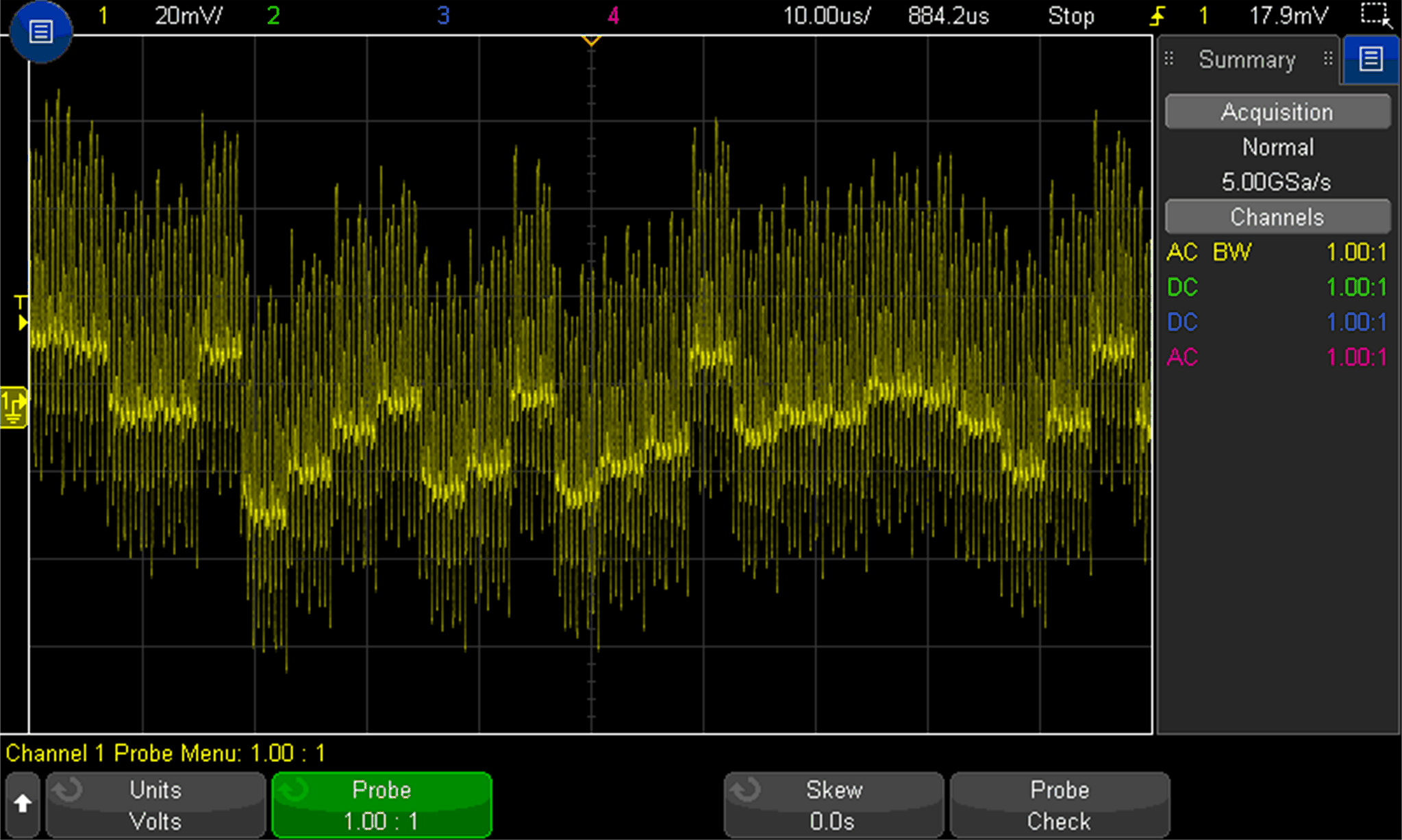
As the path to system ground becomes more complex, the effect of these artifacts becomes more apparent as added offset and noise on the output of the device. To demonstrate this, a long, discrete coiled wire was used in place of the ground plane on a TMCS1100EVM to emulate a long trace between the GND pin and system GND of the module. In addition, the bypass capacitor was also removed from the EVM to provide a worst-case look at the effects of these artifacts on the device. TMCS1100EVM With "Poor" Inductive Ground Path shows the output of the A2 device variant in this state, with no input current supplied to the device.
 Figure 3-1 TMCS1100EVM With "Poor" Inductive
Ground Path
Figure 3-1 TMCS1100EVM With "Poor" Inductive
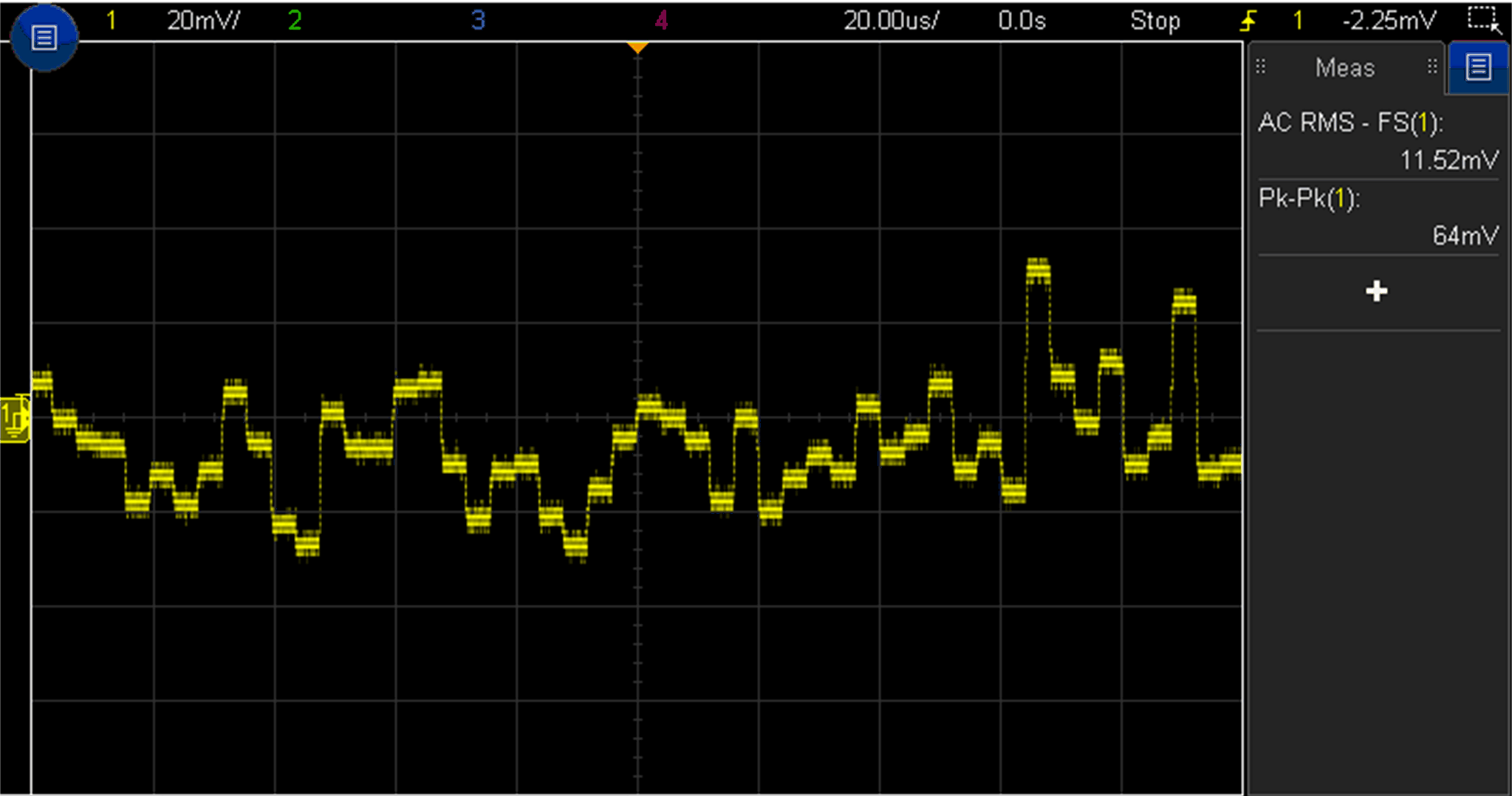
Ground PathAn ideal grounding path is a direct path from the GND pin of the device to the system GND of the board, using as wide of a trace as possible to minimize resistance and inductance between the connection points. A GND plane as used on the TMCS1100EVM is ideal. TMCS1100EVM Default "Good" Ground Path shows the output of the A1 variant under ideal grounding conditions.
 Figure 3-2 TMCS1100EVM Default "Good" Ground
Path
Figure 3-2 TMCS1100EVM Default "Good" Ground
PathNote that the "good" ground of the device still retains bouncing artifacts. This is expected as systematic noise comes from the sampling integrator used to compensate for temperature and lifetime drift, and is discussed in depth in the next section. In most designs, a wide ground plane as mentioned is not always achievable, but consideration must be given to how the device GND pin interfaces with the true ground of the system for best performance.
4 Measurement Range
4.1 Swing Limitations
Neglecting the influences of external error sources, which varies from design and operating environment, it is important to note that there are two bounds of output to examine for the device: the swing limit, and the linear operating range.
The first boundaries to consider are the swing limitations of the device. TMCS1101 Data Sheet: Swing Specifications shows the swing limitations, and demonstrates the maximum voltages that can actually be output by the device before entering a saturated condition. These bounds of output voltage for each sensing direction are determined from Equation 2 and Equation 3. The results of these equations give the range that the device is capable of measuring for the chosen operating conditions of VREF and Vs.
| PARAMETERS | TEST CONDITIONS | MIN | TYP | MAX | UNIT | |
|---|---|---|---|---|---|---|
| VOLTAGE OUTPUT | ||||||
| Swing to VS power-supply rail | RL = 10 kΩ to GND, TA= –40°C to +125°C | VS – 0.02 | VS – 0.1 | V | ||
| Swing to GND, current driven | RL = 10 kΩ to GND, TA= –40°C to +125°C | VGND + 5 | VGND + 10 | mV | ||
The second boundary, which is a smaller subset located within the swing conditions, is the linear operating range, given for each device in TMCS1101 Data Sheet: Linear Operating Region.
| PRODUCT | SENSITIVITY | ZERO CURRENT OUTPUT VOLTAGE, | IIN LINEAR MEASUREMENT RANGE | |
|---|---|---|---|---|
| ΔVOUT / ΔIIN+, IN– | VOUT,0A | VS = 5 V | VS = 3.3 V | |
| TMCS1101A1B-Q1 | 50 mV/A | 0.5 × VS | ±46 A | ±29 A |
| TMCS1101A2B-Q1 | 100 mV/A | ±23 A | ±14.5 A | |
| TMCS1101A3B-Q1 | 200 mV/A | ±11.5 A | ±7.25 A | |
| TMCS1101A4B-Q1 | 400 mV/A | ±5.75 A | – | |
| TMCS1101A1U-Q1 | 50 mV/A | 0.1 × VS | –9 A → 86 A | –5.6 A → 55.4A |
| TMCS1101A2U-Q1 | 100 mV/A | –4.5 A → 43A | –2.8 A → 27.7 A | |
| TMCS1101A3U-Q1 | 200 mV/A | –2.25 A → 21.5 A | –1.4 A → 13.85 A | |
| TMCS1101A4U-Q1 | 400 mV/A | –1.12 A → 10.75 A | – | |
This smaller subset is the range to which the sensitivity error of the device has been applied, and is ensured to operate within the data sheet specification. Care must also be taken to ensure that current levels remain below both allowable continuous DC/RMS and transient peak current safe operating areas to not exceed device thermal limits. More information on this can be found in the Safe Operating Area section of the data sheet. In short, this shows that while the TMCS1101 may be configured to work to the voltage outputs of the swing limitation, the linearity may be slightly worse at the areas of output that fall outside the linear operating range. For optimal performance, ensure that the design is kept to within the linear operating region.
See the Under the Hood: Output Swing Limitations of Current Sense Amplifiers application report for reasons behind these limitations.