How PMICs Can Help Streamline FPGA Power Design Challenges
Andrew Goodson19
System designers gain three benefits when designing systems with a field-programmable gate array (FPGA): reprogrammability, performance scalability and fast time to market. But there are also challenges that designers must overcome. In this post, I will discuss how power-management integrated circuits (PMICs) can reduce the impact of these challenges while still providing the benefits of system-power integration.
FPGAs are popular because of their reprogrammability: designers can configure the same FPGA for many different applications, and FPGAs allow design changes late in the design cycle – even after a product has been released. Although FPGAs are easy to reprogram or reconfigure, PMICs aren’t typically associated with reprogrammability. However, PMICs with external configurability can complement reprogrammability. Externally configurable devices use external hardware such as resistors and enable pins to set the default settings of the device. When you need to change the output voltage or power-up sequence, you can easily swap external components to adjust the settings.
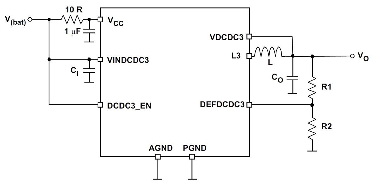
In Figure 1, the DC/DC buck converters set the output voltage using a resistor divider that connects from the output voltage to GND, and the center node of the two resistors connects to the feedback pin of the converter. This enables you to change output voltages easily without needing to reprogram the PMIC with the one-time programmable (OTP) or electrically erasable programmable read-only memory (EEPROM) settings. Additionally, each regulator has enable pins to enable startup. Simple sequencing requirements give you the flexibility to daisy-chain the regulators for power-up sequencing, while an external sequencing circuit or sequencer manages complex sequencing requirements.
 Figure 1 External Enable and Resistor
Divider for DCDC3 on the TPS65023
Figure 1 External Enable and Resistor
Divider for DCDC3 on the TPS65023TI’s Integrated Power Supply Reference Design for Xilinx Artix-7, Spartan-7 and Zynq-7000 FPGAs features a PMIC that is externally configurable such that it is easy to change the power sequencing and output voltage (Figure 2). Each regulator on the TPS65023 can be hardware-configured externally.
 Figure 2 Xilinx Artix-7, Spartan-7 and
Zynq-7000 FPGAs Reference Design Block Diagram
Figure 2 Xilinx Artix-7, Spartan-7 and
Zynq-7000 FPGAs Reference Design Block DiagramThe TPS65086100 is TI’s first customer-programmable PMIC from the TPS65086xx family. You can program the device for both prototyping samples and production units. You can also program default voltages, sequencing and general-purpose input/output (GPIO) behavior into the nonvolatile OTP memory using an MSP430™ LaunchPad™ development kit with the socketed TPS650861 BoosterPack™ plug-in module. Alternatively, you can program devices directly on the board or the TPS650860 evaluation module for testing purposes. The TPS65086100 has several example configurations for quick adaptation to some of the most popular FPGAs and multiprocessor systems on chip (MPSoCs), like the Xilinx Zynq UltraScale+ family. It also has a second reserve of OTP memory in case requirements change and you need to reprogram the device.
FPGAs enable platform scalability because their cores are scalable. In general, you can turn a high-end FPGA into a low-end one for lower-powered systems. Power solutions with built-in scalability enable the system to scale with little to no redesign. PMICs with external field-effect transistors (FETs) provide output-current scalability while allowing you to stay with the same device.
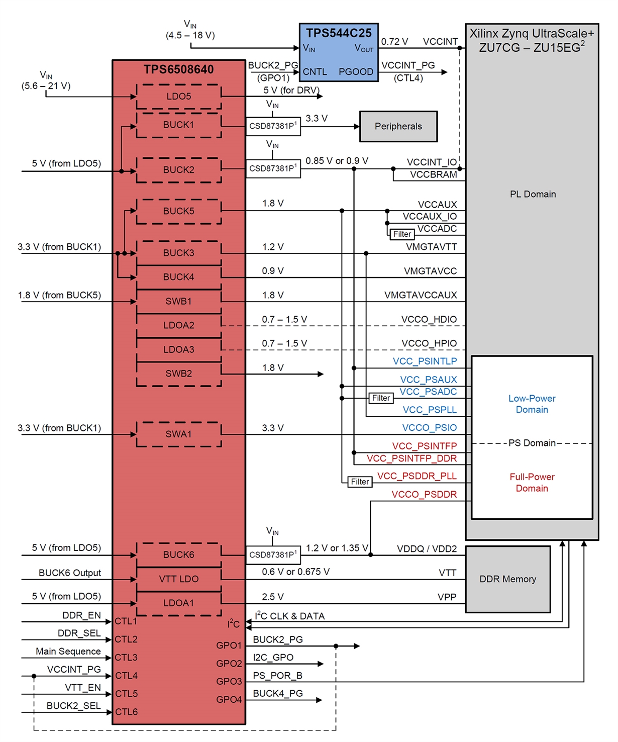
For example, Figure 3 shows how the TPS6508640 can power the Xilinx Zynq UltraScale+ ZU9EG/ZU15EG family. The TPS6508640 is a variant of the TPS65086x device, which has default sequencing and voltage settings programmed to the requirements of the Xilinx UltraScale+ ZU9EG. This device has three DC/DC controllers driving an external dual field-effect transistor (FET). Selecting the size of the FET enables you to scale the output power and maintain the same power architecture, all while powering different power levels of FPGAs.
 Figure 3 Xilinx Zynq UltraScale+ remote
radio head or backhaul block diagram
Figure 3 Xilinx Zynq UltraScale+ remote
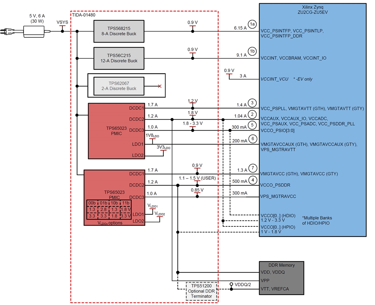
radio head or backhaul block diagramFigure 4 shows an example solution that takes scalability into account for Xilinx Zynq UltraScale+ ZU2CG/ZU5EV platforms. The TPS56C215 delivers high current (up to 12A) to the core rail of the Xilinx ZU+ MPSoC. The core rail, VCCINT, requires up to 8.7A of current for the ZU5xx variant. When using a ZU2xx/ZU4xx Xilinx variant, two TPS568215 devices reduce overall cost. You can use a TPS56C215 device or an additional TPS568215 device to meet the current needs of the application because the two buck converters are pin-to-pin equivalent.
 Figure 4 Xilinx Zynq UltraScale+
ZU2CG/ZU5EV MPSoC Block Diagram
Figure 4 Xilinx Zynq UltraScale+
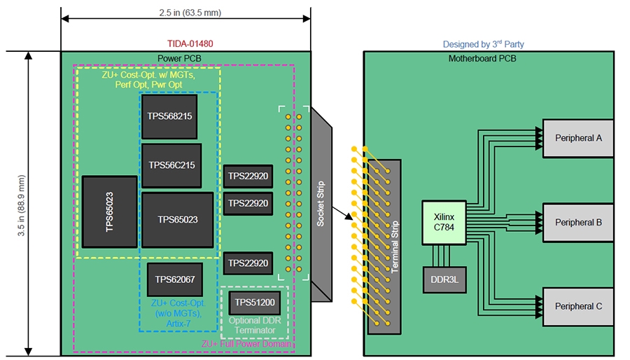
ZU2CG/ZU5EV MPSoC Block DiagramFPGAs are often used for rapid prototyping to enable quick time to market. Figure 5 shows an example of how TI reference designs for Xilinx’s Zynq UltraScale+ ZU2CG/ZU5EV MPSoCs provide solutions specifically targeted for rapid prototyping. You can focus on routing critical high-speed data and peripheral connections to ZU+ MPSoCs and let these reference designs resolve concerns related to power supply.
The motherboard on which the Xilinx ZU+ device is mounted simply needs to use the specified Samtec connectors; you can wire your printed circuit board using Xilinx terminology. You can also combine this board with your newly designed Xilinx ZU+ motherboard prototype, plug in an AC/DC (5V, 6A out) adapter to the barrel jack of the reference design and begin testing. Sample-to-production programming for the TPS65086100 speeds time to market by allowing quick tweaks in prototyping and immediate implementation of changes in production.
 Figure 5 Xilinx Zynq UltraScale+
ZU2CG/ZU5EV MPSoCs Form-factor Conceptual Drawing
Figure 5 Xilinx Zynq UltraScale+
ZU2CG/ZU5EV MPSoCs Form-factor Conceptual DrawingTI created several FPGA power solutions to help alleviate power-design challenges in your system, all while reaping the benefits of integrated power. PMICs solve challenges in designing FPGA-based systems related to reprogrammability, scalability and fast time to market.
IMPORTANT NOTICE AND DISCLAIMER
TI PROVIDES TECHNICAL AND RELIABILITY DATA (INCLUDING DATASHEETS), DESIGN RESOURCES (INCLUDING REFERENCE DESIGNS), APPLICATION OR OTHER DESIGN ADVICE, WEB TOOLS, SAFETY INFORMATION, AND OTHER RESOURCES “AS IS” AND WITH ALL FAULTS, AND DISCLAIMS ALL WARRANTIES, EXPRESS AND IMPLIED, INCLUDING WITHOUT LIMITATION ANY IMPLIED WARRANTIES OF MERCHANTABILITY, FITNESS FOR A PARTICULAR PURPOSE OR NON-INFRINGEMENT OF THIRD PARTY INTELLECTUAL PROPERTY RIGHTS.
These resources are intended for skilled developers designing with TI products. You are solely responsible for (1) selecting the appropriate TI products for your application, (2) designing, validating and testing your application, and (3) ensuring your application meets applicable standards, and any other safety, security, or other requirements. These resources are subject to change without notice. TI grants you permission to use these resources only for development of an application that uses the TI products described in the resource. Other reproduction and display of these resources is prohibited. No license is granted to any other TI intellectual property right or to any third party intellectual property right. TI disclaims responsibility for, and you will fully indemnify TI and its representatives against, any claims, damages, costs, losses, and liabilities arising out of your use of these resources.
TI’s products are provided subject to TI’s Terms of Sale (www.ti.com/legal/termsofsale.html) or other applicable terms available either on ti.com or provided in conjunction with such TI products. TI’s provision of these resources does not expand or otherwise alter TI’s applicable warranties or warranty disclaimers for TI products.
Mailing Address: Texas Instruments, Post Office Box 655303, Dallas, Texas 75265
Copyright © 2023, Texas Instruments Incorporated