DLPT030 February 2023 DLP6500FLQ , DLP650LNIR , DLP7000 , DLP7000UV , DLP9000X , DLP9000XUV , DLP9500 , DLP9500UV , DLPC410 , DLPC910
3.3 Design Details Supporting SPI Flash Configuration Method
Design details to support the Master Serial Peripheral Interface (SPI) Flash configuration with the DLPC910 and DLPC410 are as follows:
Master Serial Peripheral Interface Flash configuration mode M[2..0] pins on FPGA controllers must be changed to M[2:0] = 001.
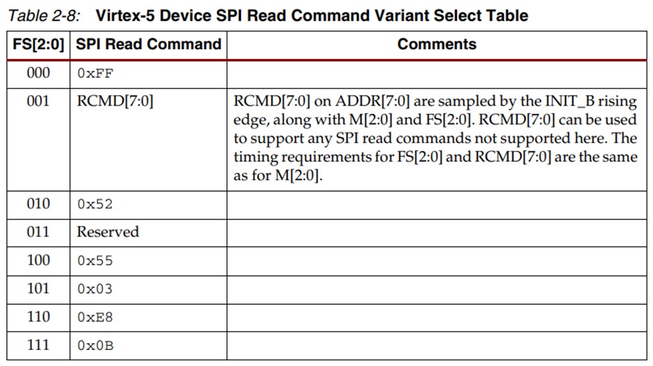
Please see page 62 of the Xilinx Virtex-5 Configuration guide UG191 for more information:FS[2:0] pins must be connected correctly to determine the type of read commands used by the SPI Flash chosen to connect to the FPGA controller. The table below (Table 2-8 in UG191 – Xilinx Virtex-5 Configuration Guide) describes the available selections:

FS2 = pin AB11 of DLPC910 Controller and DLPC410 Controller
FS1 = pin AA13 of DLPC910 Controller and DLPC410 Controller
FS0 = pin AA14 of DLPC910 Controller and DLPC410 Controller