DLPT030 February 2023 DLP6500FLQ , DLP650LNIR , DLP7000 , DLP7000UV , DLP9000X , DLP9000XUV , DLP9500 , DLP9500UV , DLPC410 , DLPC910
3.4 SPI Flash Layout Connections
.
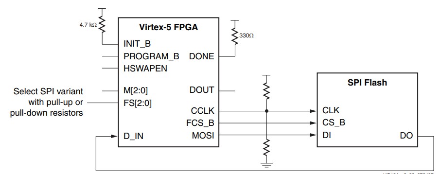
SPI Flash Write Protect (WP#) should be pulled high to allow for programming through the Virtex 5 JTAG interface. SPI Flash Reset (RESET#) or Hold (HOLD#) should be pulled high to prevent the SPI Flash from pausing serial communications with the DLPC410 and DLPC910 controllers.
For additional details on how the SPI Configuration Flash is connected to the DLPC410 Controller and DLPC910 Controller, please refer to the schematics for the DLPLCRC910EVM and DLPLCRC410EVM.
- FCS_B = pin AA10 of DLPC910 Controller and DLPC410 Controller
- MOSI = pin AA9 of DLPC910 Controller and DLPC410 Controller
- CCLK = pin J10 of DLPC910 Controller and DLPC410 Controller
- D_IN = pin K11 of DLPC910 Controller and DLPC410 Controller