SBOA615 November 2024 INA180 , INA180-Q1 , INA181 , INA181-Q1 , INA183 , INA185 , INA185-Q1 , INA186 , INA186-Q1 , INA190 , INA190-EP , INA190-Q1 , INA191 , INA199 , INA199-Q1 , INA209 , INA210 , INA210-Q1 , INA211 , INA211-Q1 , INA212 , INA212-Q1 , INA213 , INA213-Q1 , INA214 , INA214-Q1 , INA215 , INA215-Q1 , INA216 , INA2180 , INA2180-Q1 , INA2181 , INA2181-Q1 , INA219 , INA2191 , INA220 , INA220-Q1 , INA223 , INA225 , INA225-Q1 , INA226 , INA226-Q1 , INA228 , INA228-Q1 , INA229 , INA229-Q1 , INA2290 , INA230 , INA231 , INA232 , INA233 , INA234 , INA236 , INA237 , INA237-Q1 , INA238 , INA238-Q1 , INA239 , INA239-Q1 , INA240 , INA240-Q1 , INA241A , INA241A-Q1 , INA241B , INA241B-Q1 , INA250 , INA250-Q1 , INA253 , INA253-Q1 , INA254 , INA260 , INA280 , INA280-Q1 , INA281 , INA281-Q1 , INA290 , INA290-Q1 , INA293 , INA293-Q1 , INA296A , INA296A-Q1 , INA296B , INA296B-Q1 , INA300 , INA300-Q1 , INA301 , INA301-Q1 , INA302 , INA302-Q1 , INA303 , INA303-Q1 , INA310A , INA310A-Q1 , INA310B , INA310B-Q1 , INA3221 , INA3221-Q1 , INA381 , INA381-Q1 , INA4180 , INA4180-Q1 , INA4181 , INA4181-Q1 , INA4230 , INA4235 , INA4290 , INA700 , INA740A , INA740B , INA745A , INA745B , INA750B , INA780A , INA780B , INA790B , INA791B , LMP8278Q-Q1 , LMP8601 , LMP8601-Q1 , LMP8602 , LMP8602-Q1 , LMP8603 , LMP8603-Q1 , LMP8640 , LMP8640-Q1 , LMP8640HV
- 1
- Abstract
- Trademarks
- 1Introduction
- 2What is ESD, EOS, and Latch Up?
- 3Risky Applications for Current Sense Amplifiers
- 4Summary
- 5References
3.4 Applications that Float the Supply (VS or GND) Pins of CSA
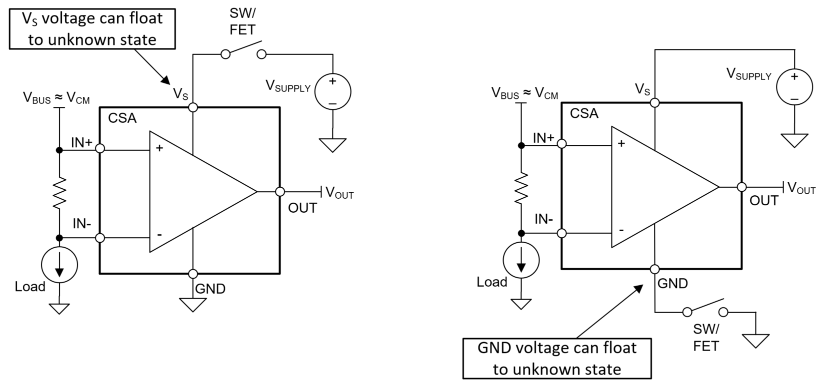
In general, TI does not recommend to ever float the supply pins of a CSA usually with a switch or FET due to the inherent risk of latch up as shown in Figure 3-6. A designed for VS needs to be driven to GND when turned off and when this is the case, there is no required power sequence for CSA. VS and IN+/IN- can be turned on or off independently of each other.
This latch up can occur when input pins (IN+ and IN-) are connected to a voltage (bus is on) and a floating VS or GND suddenly switched through a FET or physically connected to analog source. This can be referred to as hot-plugging or hot-swapping. This scenario presents two fundamental issues:
- When VS is floating and input pins are connected to a live bus voltage, the CSAs VS pin can float to some unknown state, usually up to 1V above GND pin.
- When the hot-plug occurs, this generates a very noisy and uncontrolled charge circuit.
 Figure 3-6 Avoid Floating Supply Pins
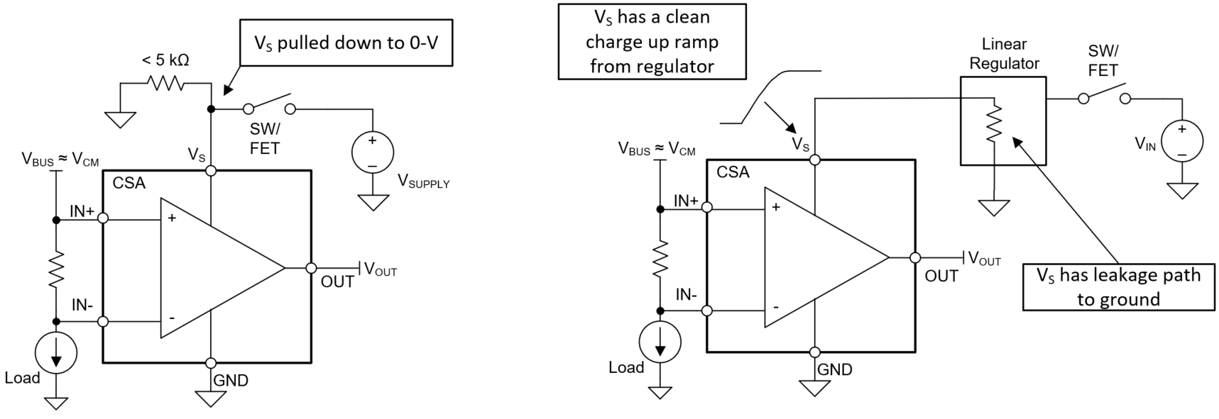
For many engineers, there are advantages to turn off a CSA for overall system power reduction and thus a FET to open up VS is enticing. If an engineer does pursue this method, then the best practice is to place a 5kΩ resistor from VS pin to GND pin as illustrated in Figure 3-7. This pull-down resistor can act as a soft-ground for Vs pin and keep Vs in a determined state as well as provide a path for sudden current discharge when FET turns on.
Note that the usual case of powering a CSA with an LDO is shown in Figure 3-7 to illustrate that LDO usually have some small leakage current to ground when disabled and also have stable voltage turn on.
 Figure 3-7 Acceptable Supply Disable/Enable
Floating the GND pin is not a good idea unless your system has control over power sequencing and opening/closing all pins of the device (including digital pins for digital power monitors), which usually is not be practical. In general, the GND pin needs to be the first pin connected to a system and the last pin disconnected from a system. Basically, you can think of opening/closing a ground pin as how you connect the pins of an EVM (evaluation module) to a bench set up.