SLAAE75A November 2022 – March 2023 MSPM0L1105 , MSPM0L1106 , MSPM0L1227 , MSPM0L1228 , MSPM0L1228-Q1 , MSPM0L1303 , MSPM0L1304 , MSPM0L1304-Q1 , MSPM0L1305 , MSPM0L1305-Q1 , MSPM0L1306 , MSPM0L1306-Q1 , MSPM0L1343 , MSPM0L1344 , MSPM0L1345 , MSPM0L1346 , MSPM0L2227 , MSPM0L2228 , MSPM0L2228-Q1
1 MSPM0L Hardware Design Check List
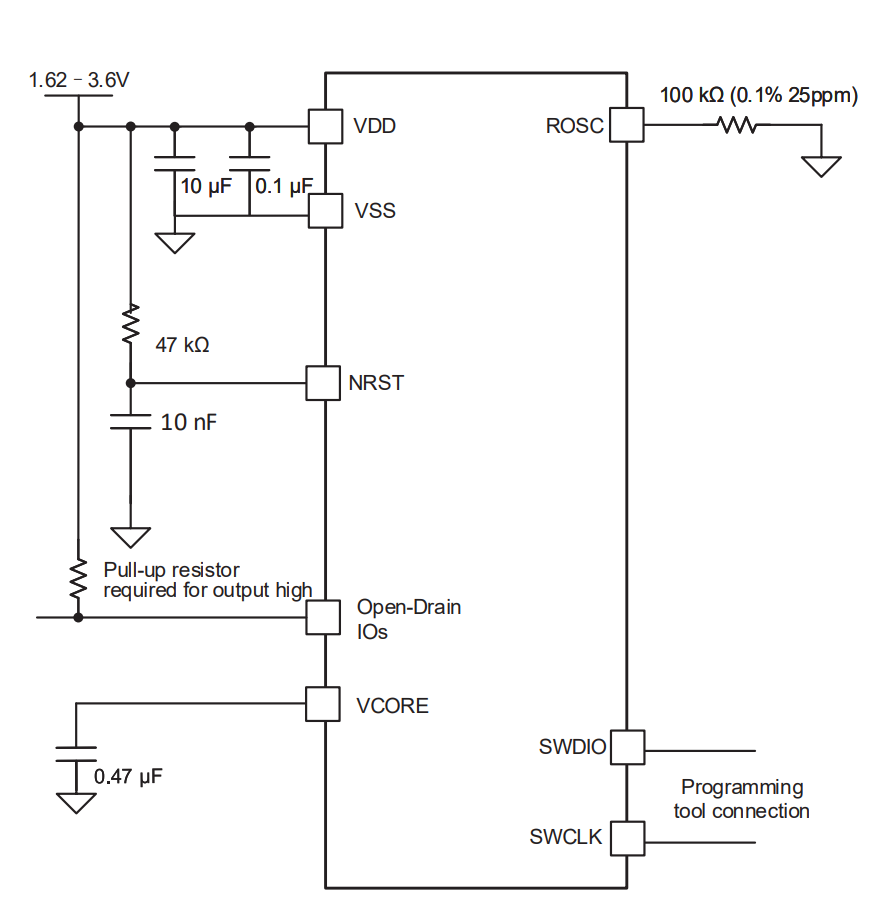
#GUID-0388845E-77CD-4FEF-AB17-597547F7F425/GUID-9D414E7A-A6E4-4DCE-A5B5-9492C6B1C56D describes the main signal that needs to be checked during the MSPM0L hardware design process. The following sections give more details.
| Pin (1) | Description | Requirements |
|---|---|---|
| VDD | Power supply positive pin | Place 10-µF and 100-nF capacitors between VDD and VSS, and keep those part close to VDD and VSS. |
| VSS | Power supply negative pin | |
| VCORE | Core voltage (typical: 1.35 V) | Connect a 470-nF capacitor to VSS, do not supply any voltage or apply any external load to the VCORE pin. |
| NRST | Reset pin | Connect an external 47-kΩ pullup resistor with a 10-nF pulldown capacitor. |
| ROSC | External reference resistor pin |
|
| VREF+ | Voltage reference power supply for external reference input |
|
| VREF- | Voltage reference ground supply for external reference input | |
| SWCLK | Serial wire clock from debug probe | Internal pullup to VDD, does not need any external part. |
| SWDIO | Bidirectional (shared) serial wire data | Internal pulldown to VSS, does not need any external part. |
| PA0, PA1 | Open-drain I/O | Pull-up resistor required for output high |
| PA18 | Default BSL invoke pin | Keep pulled down to avoid entering BSL mode after reset. The BSL invoke pin can be remapped. |
| PAx (exclude PA0, PA1) | General-purpose I/O | Set corresponding pin functions to GPIO (PINCMx.PF = 0x1) and configure unused pins to output low or input with internal pullup or pulldown resistor. |
| OPAx_IN0-(2) | OPAx inverting terminal input 0 | This pin is high-impedance, does not need any external part if unused. |
TI recommends connecting a combination of a 10-μF and a 0.1-nF low-ESR ceramic decoupling capacitor to the VDD and VSS pins . Higher-value capacitors can be used but can impact supply rail ramp-up time. Decoupling capacitors must be placed as close as possible to the pins that they decouple (within a few millimeters).
The NRST reset pin is required to connect an external 47-kΩ pullup resistor with a 10-nF pulldown capacitor.
The SYSOSC frequency correction loop (FCL) circuit utilizes an external 100-kΩ resistor, populated between the ROSC pin and VSS, to stabilize the SYSOSC frequency by providing a precision reference current for the SYSOSC. This resistor is not required if the SYSOSC FCL is not enabled.
A 0.47-µF tank capacitor is required for the VCORE pin and must be placed close to the device with minimum distance to the device ground.
For 5-V-tolerant open drain (ODIO), a pullup resistor is required to output high, this is required for I2C and UART functions if the ODIO are used.
 Figure 1-1 MSPM0L Typical Application Schematic