SLAAE75A November 2022 – March 2023 MSPM0L1105 , MSPM0L1106 , MSPM0L1227 , MSPM0L1228 , MSPM0L1228-Q1 , MSPM0L1303 , MSPM0L1304 , MSPM0L1304-Q1 , MSPM0L1305 , MSPM0L1305-Q1 , MSPM0L1306 , MSPM0L1306-Q1 , MSPM0L1343 , MSPM0L1344 , MSPM0L1345 , MSPM0L1346 , MSPM0L2227 , MSPM0L2228 , MSPM0L2228-Q1
5.2 Debug Port Connection With Standard JTAG Connector
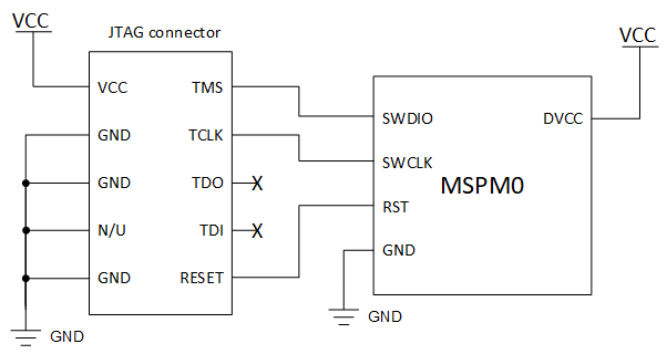
#FIG_Z4Q_RGC_GVB shows the connection between MSPM0L family MCU SWD debug port with the standard JTAG connector.
 Figure 5-3 JTAG and MSPM0L Connection
For MSPM0L device, you can use XDS110 to implement debug/download function. Here list the contents of the XDS110 and provides instruction on installing the hardware.
Standard XDS110
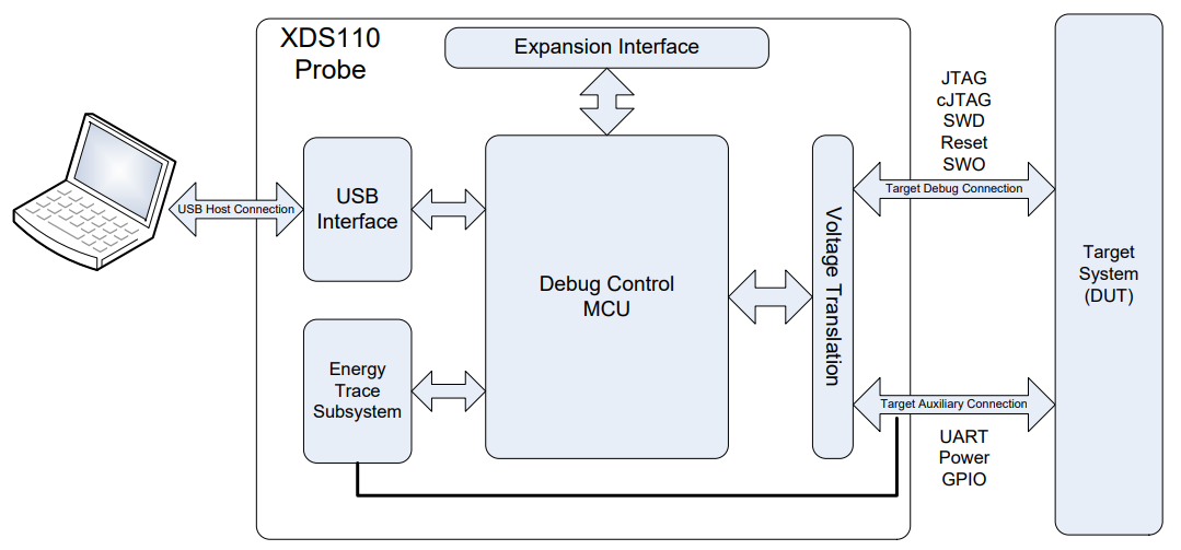
You can purchase a standard XDS110 in ti.com. #FIG_V2Y_CHC_GVB shows a high-level diagram of the major functional areas and interfaces of the XDS110 probe.
 Figure 5-4 XDS110 Probe High-Level Block Diagram
More standard XDS110 information, see the XDS110 Debug Probe User's Guide.
Lite XDS110 (MSPM0 LaunchPad™ kit)
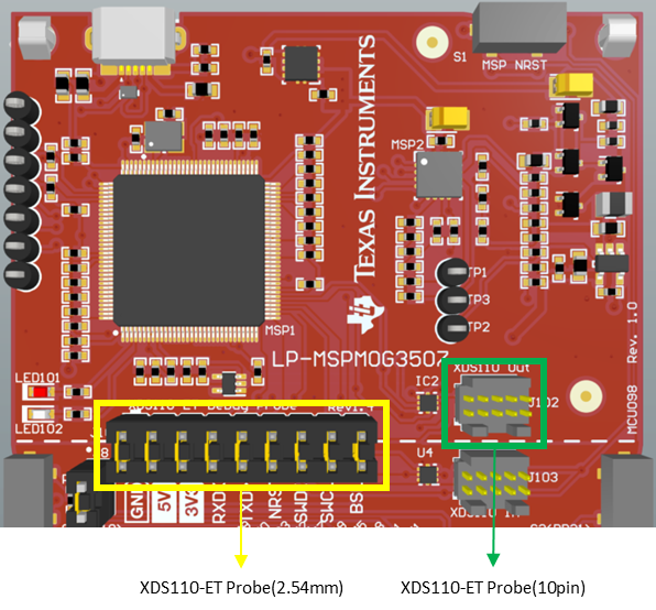
The MSPM0 LaunchPad kit include the XDS110-ET (Lite) circuit. You can also use this debugger to download your firmware into MSPM0 device. #FIG_NZV_3HC_GVB shows the XDS110-ET circuit.
There are two probes in XDS110-ET:
2.54-mm probe: This port supports the SWD protocol and includes a 5-V or 3.3-V power supply. You can connect SWDIO SWCLK 3V3 GND to the board and download firmware into the MSPM0L device.
This probe supports EnergyTrace™ technology so you can use this circuit to measure power consumption precisely in real time.
More information on EnergyTrace technology, visit the EnergyTrace Technology tool page.
 Figure 5-5 XDS110-ET Circuit
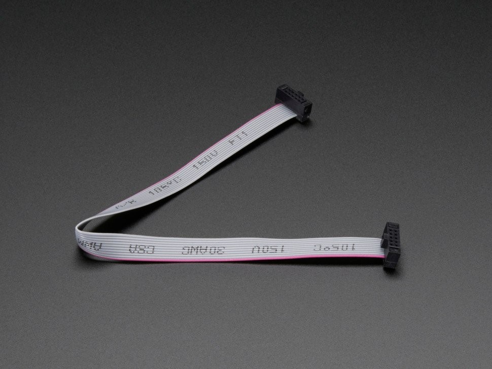
10-pin probe: This port supports the JTAG and SWD protocols and include a 3.3-V power supply. You can use the 10-pin cable to connect the board and XDS110-ET and download firmware into the MSPM0L device. #FIG_FJ1_LHC_GVB show the 10-pin cable.
 Figure 5-6 Arm Standard 10-Pin Cable
- Standard XDS110 support level shift for debug ports, XDS110-ET just support 3.3v probe level.
- TI does not recommend using the XDS110 to power other devices except the MSPM0L MCU. The XDS110 integrates an LDO with limited current drive capability.
- XDS110-ET 2.54-mm probe does not support the JTAG protocol.
- XDS110-ET 10-pin probe does not support EnergyTrace technology.