SLAAE75A November   2022  – March 2023 MSPM0L1105 , MSPM0L1106 , MSPM0L1303 , MSPM0L1304 , MSPM0L1304-Q1 , MSPM0L1305 , MSPM0L1305-Q1 , MSPM0L1306 , MSPM0L1306-Q1 , MSPM0L1343 , MSPM0L1344 , MSPM0L1345 , MSPM0L1346


  1.   Abstract
  2.   Trademarks
  3. MSPM0L Hardware Design Check List
  4. Power Supplies in MSPM0L Devices
    1. 2.1 Digital Power Supply
    2. 2.2 Analog Power Supply
    3. 2.3 Built-in Power Supply and Voltage Reference
    4. 2.4 Recommended Decoupling Circuit for Power Supply
  5. Reset and Power Supply Supervisor
    1. 3.1 Digital Power Supply
    2. 3.2 Power Supply Supervisor
  6. Clock System
    1. 4.1 Internal Oscillators
    2. 4.2 External Clock Output (CLK_OUT)
    3. 4.3 Frequency Clock Counter (FCC)
  7. Debugger
    1. 5.1 Debug Port Pins and Pinout
    2. 5.2 Debug Port Connection With Standard JTAG Connector
  8. Key Analog Peripherals
    1. 6.1 ADC Design Considerations
    2. 6.2 OPA Design Considerations
    3. 6.3 DAC Design Considerations
    4. 6.4 COMP Design Considerations
    5. 6.5 GPAMP Design Considerations
  9. Key Digital Peripherals
    1. 7.1 Timer Resources and Design Considerations
    2. 7.2 UART and LIN Resources and Design Considerations
    3. 7.3 I2C and SPI Design Considerations
  10. GPIOs
    1. 8.1 GPIO Output Switching Speed and Load Capacitance
    2. 8.2 GPIO Current Sink and Source
    3. 8.3 High Speed GPIOs
    4. 8.4 Open-Drain GPIOs Enable 5-V Communication Without a Level Shifter
    5. 8.5 Communicate With 1.8-V Devices Without a Level Shifter
    6. 8.6 Unused Pins Connection
  11. Layout Guides
    1. 9.1 Power Supply Layout
    2. 9.2 Considerations for Ground Layout
    3. 9.3 Traces, Vias, and Other PCB Components
    4. 9.4 How to Select Board Layers and Recommended Stack-up
  12. 10Bootloader
    1. 10.1 Bootloader Introduction
    2. 10.2 Bootloader Hardware Design Considerations
      1. 10.2.1 Physical Communication interfaces
      2. 10.2.2 Hardware Invocation
  13. 11References
  14. 12Revision History

Frequency Clock Counter (FCC)

The frequency clock counter (FCC) enables flexible in-system testing and calibration of a variety of oscillators and clocks on the device. The FCC counts the number of clock periods seen on the selected source clock within a known fixed trigger period (derived from a secondary reference source) to provide an estimation of the frequency of the source clock.
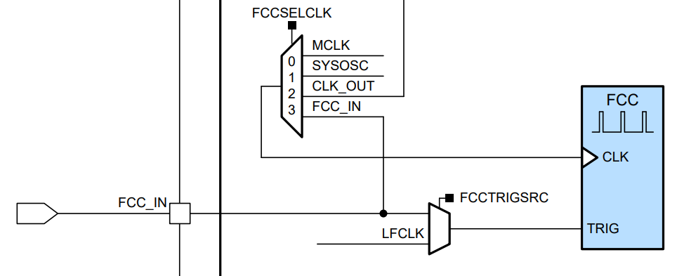
GUID-43B2BFA6-89F4-406A-9CDE-DCD90BDA96A1-low.png Figure 4-4 MSPM0L Series Frequency Clock Counter Block Diagram

Application software can use the FCC to measure the frequency of the following oscillators and clocks:

  • MCLK
  • SYSOSC
  • CLK_OUT
  • The external FCC input (FCC_IN)
Note: While the external FCC input (FCC_IN function) can be used as either the FCC clock source or the FCC trigger input, it cannot be used for both functions during the same FCC capture. It must be configured as either the FCC clock source or the FCC trigger.