SLAAE75A November 2022 – March 2023 MSPM0L1105 , MSPM0L1106 , MSPM0L1227 , MSPM0L1228 , MSPM0L1228-Q1 , MSPM0L1303 , MSPM0L1304 , MSPM0L1304-Q1 , MSPM0L1305 , MSPM0L1305-Q1 , MSPM0L1306 , MSPM0L1306-Q1 , MSPM0L1343 , MSPM0L1344 , MSPM0L1345 , MSPM0L1346 , MSPM0L2227 , MSPM0L2228 , MSPM0L2228-Q1
9.2 Considerations for Ground Layout
System ground is the most critical area and foundation related to noise and EMI problems on the board. The most practical way to minimize these problems is to have a separate ground plane.
What is Ground Noise?
Each signal originating from a circuit (say Driver) has a return current flow to its source via ground path. As the frequency increases, or even for simple but high-current switching like relays, there is a voltage drop due to line impedance generating interference in the grounding scheme. The return path is always via the least resistance. For DC signals, that will be the lowest resistive path and for high frequency signals it will be the lowest impedance path. This explains how a ground plane simplifies the issue and is the key to ensuring signal integrity.
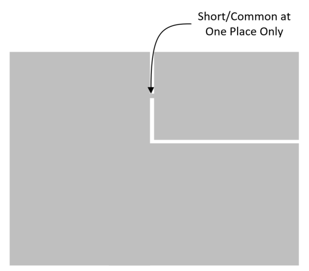
It is not recommended that the digital return signals propagate inside the analog return (ground) area; therefore, split the ground plane to keep all the digital signal return loops within its ground area. This splitting should be done carefully. Many designs use a single (common) voltage regulator to generate a digital and analog supply of the same voltage level (for example, 3.3 V). Isolate the analog rail and digital supply rails and their respective grounds from each other. Be careful while isolating ground, as both grounds have to be shorted somewhere. #GUID-368DEC56-5B50-4DF2-AD65-BD393D641849 shows how possible return paths for digital signals are not allowed to form a loop passing through the analog ground. On each design, decide the common point considering the component placements and so forth. Do not add any inductors (ferrite bead) or resistors (not even zero Ω) in the series with any ground trace. The impedance increases due to associated inductance at a high frequency, causing a voltage differential. Do not route a signal referenced to digital ground over analog ground or the other direction.
 Figure 9-2 Digital and Analog Grounds and Common Area