SLUAAY2 December 2024 ISO5451 , ISO5451-Q1 , ISO5452 , ISO5452-Q1 , ISO5851 , ISO5851-Q1 , ISO5852S , ISO5852S-EP , ISO5852S-Q1 , UCC21710 , UCC21710-Q1 , UCC21717-Q1 , UCC21732 , UCC21732-Q1 , UCC21736-Q1 , UCC21737-Q1 , UCC21738-Q1 , UCC21739-Q1 , UCC21750 , UCC21750-Q1 , UCC21755-Q1 , UCC21756-Q1 , UCC21759-Q1
4.2 Short Circuit Voltage-Based Protection Implementation
Short-circuit voltage-based protection is typically done using the DESAT function in a gate driver. OC-detection approach is also sometimes used for voltage-based protection. So the two options are:
- VSC voltage detection across FET using DESAT pin
- VSC voltage detection across FET using OC pin
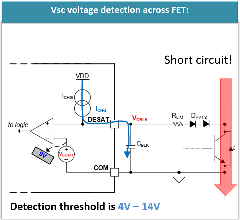
Option1: VSC voltage detection across FET using DESAT pin:
 Figure 4-4 DESAT Circuit Implementation
for VSC Voltage Detection
Figure 4-4 DESAT Circuit Implementation
for VSC Voltage DetectionThe typical voltage detection approach across the power module is using the DESAT node as shown in Figure 4-4. The high voltage drain node is connected through 1 or 2 high voltage diodes and a current limiting resistor (RLIM) to the DESAT pin. A blanking capacitor (CBLK) is connected in the DESAT pin as well. DESAT node has an internal current source, internally connected to the VDD bias (secondary isolated bias). When INP is high, the internal current source will supply the (ICHG) current through the DESAT pin. The current source path is not active when INP is low.
During normal operation, the voltage across the power module is low, hence the high-voltage diodes (DHV 1, 2) are forward biased and the current flows through the diode and power module. However, during short-circuit events, the voltage across the power module is high, which causes the DHV1, 2 to be reverse biased; hence the DESAT current path is disconnected. So, the ICHG charges the CBLK capacitor. When the voltage on the DESAT pin exceeds the detection threshold, it triggers the DESAT fault and turns the gate driver output off to protect the system. The turn-off operation is discussed in a separate section as the turn off operation needs special consideration due to high di/dt involved during the SC/OC event.
The gate driver's internal current source is typically around 500μA-2mA. To enable faster protection, an external current source path can be planned by connecting the DESAT node to VDD/OUTH with a resistor. The same concept can be used for OC pin as well.
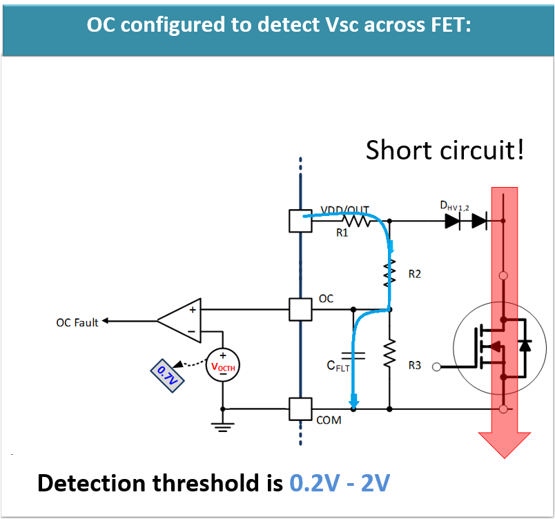
Option2: VSC voltage detection across FET using OC pin
 Figure 4-5 OC Pin Circuit Implementation
for VSC Voltage Detection
Figure 4-5 OC Pin Circuit Implementation
for VSC Voltage DetectionOC pin is typically used to sense current as explained in the current-based protection section. However, the OC pin can be used for VSC-based voltage detection as well by planning the current source from VDD/OUT as shown in Figure 4-5. Similar to the DESAT concept, during normal operation, the VDD/OUT charge current path is through the power module, and during the OC/SC event, the current path is through the CFLT capacitor and triggers the OC event.
VSC- and ISC-based protection approaches explained using the DESAT or OC pin. The ISC-based protection approach is faster, however, causes increased power loss in the case of the Rshunt approach or needed power module with sense pin for the Rsense approach. Due to these reasons, it is very common practice to use DESAT-based approach for both of the SiC and IGBT modules. In this application note, data has been collected based on the VSC approach for both DESAT and OC pin.