SLUUC66B May 2020 – April 2021 TPSM5D1806
1 Getting Started
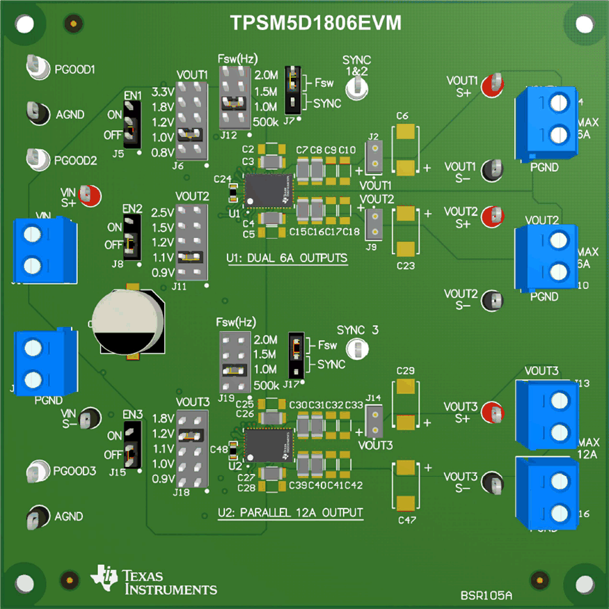
Figure 1-1 highlights the user interface items associated with the EVM. The VIN and PGND terminal blocks (J1 and J3) are used for connection to the host input supply and the VOUT and PGND terminal blocks (J4, J10, J13, J16) are used for connection to the load. These terminal blocks can accept up to 16-AWG wire.
Table 1-1 TPSM5D1806EVM Operating
Range
| Device | Output Voltage | Output Current Range | Input Voltage |
|---|---|---|---|
| U1 Dual Output | VOUT1 = 0.8 V, 1.0 V, 1.2 V, 1.8 V, or 3.3 V | 0 to 6 A per output | VIN = 4.5 V to 15 V |
| VOUT2 = 0.9 V, 1.1 V, 1.2 V, 1.5 V, or 2.5 V | |||
| U2 Parallel Output | VOUT3 = 0.9 V, 1.0 V, 1.1 V, 1.2 V, or 1.8 V | 0 to 12 A |
 Figure 1-1 EVM User Interface
- The VIN S+ and VIN S- input voltage test points as well as the VOUT S+ and VOUT S- output voltage test points, located near the power terminal blocks are intended to be used as voltage monitoring points where voltmeters can be connected to measure VIN and VOUT. Do not use these S+ and S- monitoring test points as the input supply or output load connection points. The PCB traces connecting to these test points are not designed to support high currents.
- The VOUT1 (J2), VOUT2 (J9) and VOUT3 (J14) scope sockets can be used to monitor VOUT waveforms with an oscilloscope. These test points are intended for use with un-hooded scope probes outfitted with a low-inductance ground lead (ground spring) mounted to the scope probe barrel. The two sockets of each test point are on 0.1 inch centers. The scope probe tip should be inserted into the socket marked with a white dot printed on the board and the scope ground lead should be inserted into the other socket.
- The control test points located around the device are made available to test the features of the device. Refer to Section 2 for more information on the individual control test points.
- The VOUT jumpers (J6, J11, J18) and FSW jumpers (J12, J19) are provided to select the desired output voltage and appropriate switching frequency. The Fsw/SYNC jumpers (J7, J17) are provided to select the desired switching frequency method, either to an external clock (SYNC) or the switching frequency (Fsw) selected by the FSW jumpers. Before applying power to the EVM, make sure that the jumpers are present and properly positioned for the intended output voltage. Always remove input power before changing the jumper settings.