SLVAE30E February 2021 – March 2021 TPS1H000-Q1 , TPS1H100-Q1 , TPS1H200A-Q1 , TPS1HA08-Q1 , TPS25200-Q1 , TPS27S100 , TPS2H000-Q1 , TPS2H160-Q1 , TPS2HB16-Q1 , TPS2HB35-Q1 , TPS2HB50-Q1 , TPS4H000-Q1 , TPS4H160-Q1
- Trademarks
- 1Introduction
- 2Driving Resistive Loads
- 3Driving Capacitive Loads
- 4Driving Inductive Loads
- 5Driving LED Loads
- 6Appendix
- 7References
- 8Revision History
3.3.3 Thermal Dissipation
With large capacitive loads there are thermal considerations in the Smart High Side Switch during current limiting that must be considered. While the capacitor is charging, the Smart High Side Switch limits IINRUSH by regulating the gate voltage of the MOSFET inside of the Smart High Side Switch.
Lets refer back to Equation 25 for charging a capacitor.

For a regulated constant IINRUSH, the capacitor needs to see a constant dVCAP/dT . This means the voltage must linearly increase across the capacitor rather than the near instantaneous voltage increase that occurs with no current limiting. The voltage applied over the capacitor is VCAP and is shown in Equation 20.

With a constant VSUPPLY, Equation 20 shows that if VCAP increases linearly, VDS must be the inverse of VCAP and decrease linearly. Therefore, for a constant current capacitive charging the Smart High Side Switch VDS will initially be equal to VSUPPLY before dropping towards zero while VCAP simultaneously increases to reach VSUPPLY. Figure 3-11 shows this behavior with the TPS2H160-Q1 driving a large (470µF) capacitive load to 24V with a current limit of 500mA.
 Figure 3-11 VDS While Charging Capacitance
We see the Smart High Side Switch limiting the output current to 500mA as the OUT1 voltage over the capacitance linearly increases from 0V to 24V and the VDS slowly decreases inversely from the supply voltage towards 0V.
During this charging period the power dissipation, PDIS, in the Smart High Side Switch is calculated in Equation 21.

The current is now limited and no longer unchecked inrush current so the equations will now consider ILIM rather than IINRUSH. Since ILIM is constant and initially VDS = VSUPPLY, the peak power dissipation occurs at the beginning of the pulse and is given in Equation 22.

When the capacitor is fully charged, VDS ≈ 0 so PDIS ≈ 0. For a first approximation this means that the average power dissipation during the charging period is given in Equation 23.

This average dissipation will occur for a period equal to the charging period which is calculated in Equation 24.

In Figure 3-11 we see a peak power dissipation of 24V × 500mA = 12W, an average dissipation of 6W, and a charging time of 22.9ms. In order to have reliable operation the FET must be able to dissipate this heat over the charging time.
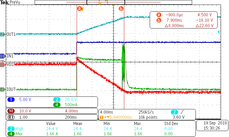
Lets look at what happens in Figure 3-12 when the current limit is increased to 1A.
 Figure 3-12 TPS2H160-Q1 Charging at 1A
The peak power dissipation has increased to 24W and the average dissipation to 12W, however the charging time has decreased to 8.8 ms. A higher current limit equates to a higher peak power dissipation with a shorter pulse while a lower current limit equates to a low peak dissipation for a longer time.