SNAA411 September 2024 CDCLVC1102 , CDCLVC1103 , CDCLVC1104 , CDCLVC1110 , CDCLVD1204 , LMK00301 , LMK00304 , LMK00306 , LMK00308 , LMK01801 , LMK04832 , LMK1C1102 , LMK1C1103 , LMK1C1104 , LMK1C1106 , LMK1C1108 , LMK1D1204 , LMK1D1208 , LMX2485 , LMX2491 , LMX2572 , LMX2592 , LMX2594 , LMX2595 , LMX2820
6.1 LMK1C110x Additive Noise vs Others
As described in Section 5.1 that noise measurement equipment can give optimistic results for additive phase noise results due to slew rate issue. An alternative cascaded setup is used to model the actual additive phase noise of LMK1C110x vs competition's best performing buffer. We use cascaded buffers and treat the first buffer as source. Phase noise setup for the buffer is shown in Figure 6-2
 Figure 6-2 Additive Noise Buffer
Setup
Figure 6-2 Additive Noise Buffer
SetupFollowing additive phase noise plots compare the performance of TI buffer vs competition.
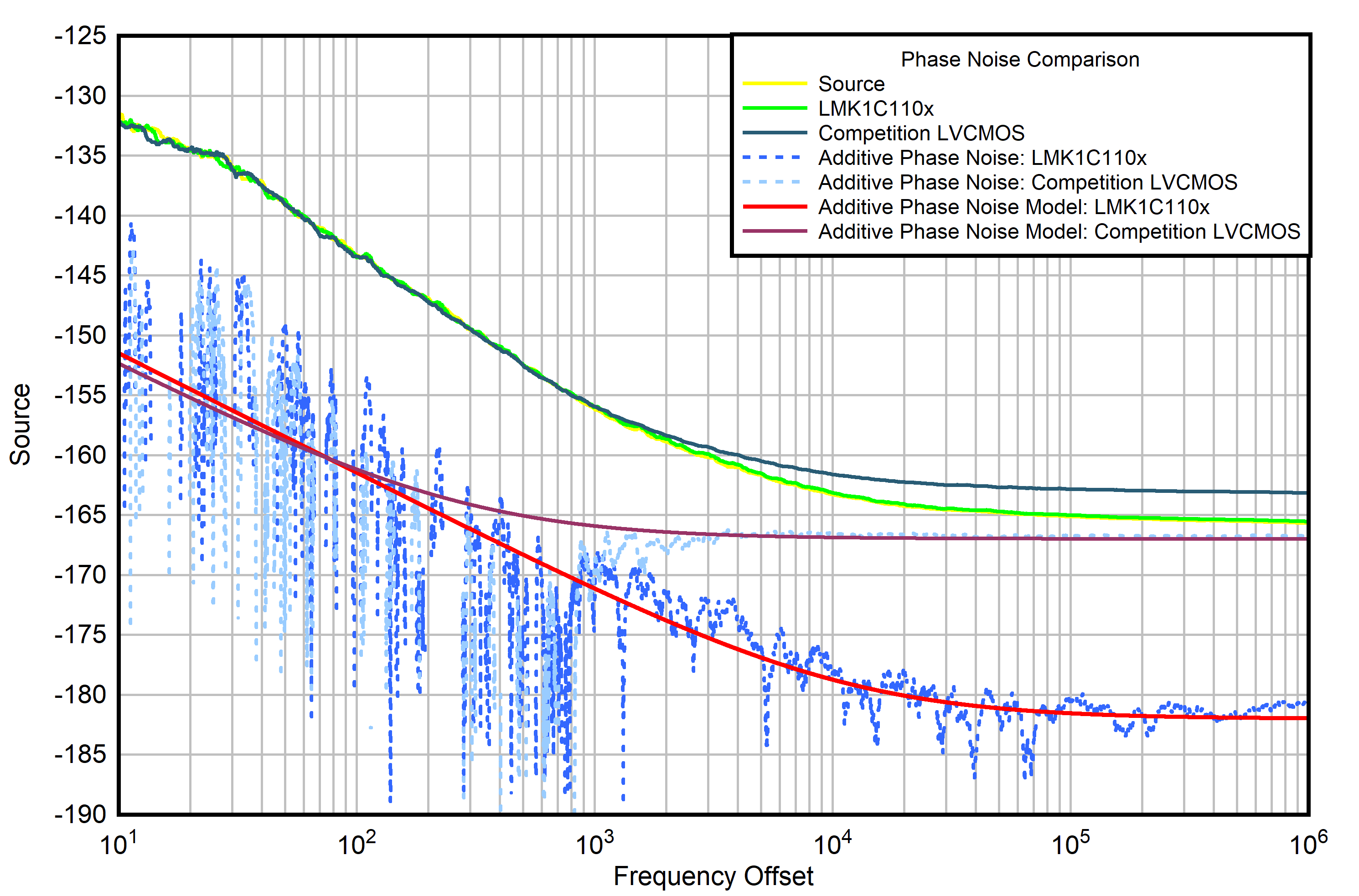
 Figure 6-3 Total Phase Noise at 10MHz
Output
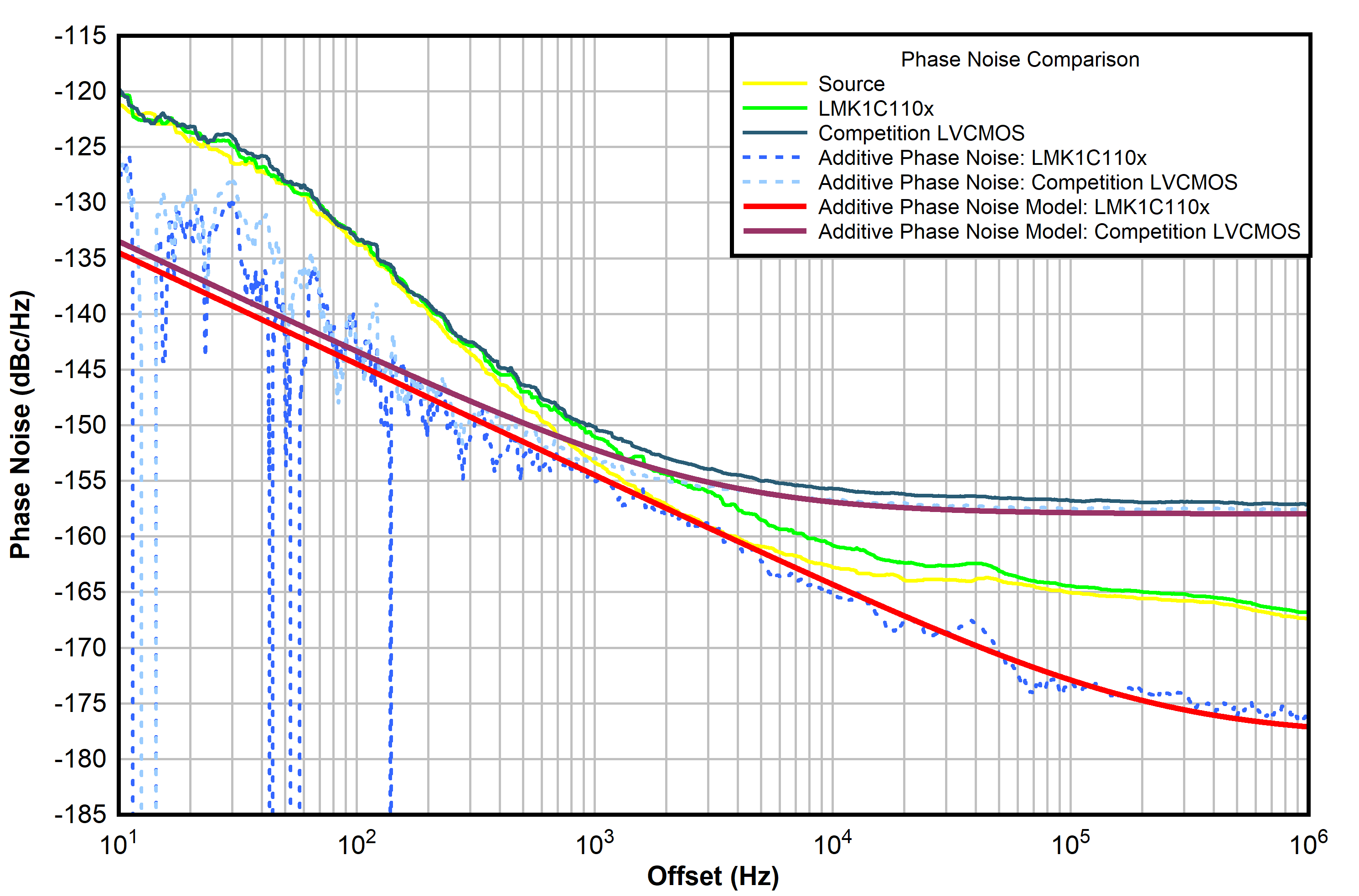
 Figure 6-5 Total Phase Noise at
100MHz Output
 Figure 6-7 RMS Jitter (12kHz - 1MHz):
10MHz Output - LMK1C110x vs Competition
  Figure 6-9 RMS Jitter (12kHz -
20MHz): 100MHz Output - LMK1C110x vs Competition
| Noise Floor = –181.9dBc/Hz, 1/f Noise = 178.5dBc/Hz at 10kHz |

| Noise Floor = –177.9dBc/Hz, 1/f Noise = –164.3dBc/Hz at 10kHz |
 Figure 6-8 RMS Jitter (10Hz - 1MHz):
12MHz Output - LMK1C110x vs Competition
 Figure 6-10 RMS Jitter (10Hz - 50MHz):
100MHz Output - LMK1C110x vs Competition
Figure 6-10 RMS Jitter (10Hz - 50MHz):
100MHz Output - LMK1C110x vs Competition| Parameter | LMK1C110x | Competition LVCMOS | Unit | ||
|---|---|---|---|---|---|
| Frequency | 10MHz | 100MHz | 10MHz | 100MHz | fs |
| Additive Jitter (10Hz - 1MHz) | 21.87 | - | 104.82 | - | |
| Additive Jitter (12kHz - 1MHz) | 21.39 | - | 104.41 | - | |
| Additive Jitter (12kHz - 20MHz) | - | 4.51 | - | 133.35 | |
| Additive Jitter (10Hz - 50MHz) | - | 16.38 | - | 200.90 | |