SPRACV0A February 2021 – March 2023 F29H850TU , F29H850TU , F29H859TU-Q1 , F29H859TU-Q1 , TMS320F2800132 , TMS320F2800132 , TMS320F2800133 , TMS320F2800133 , TMS320F2800135 , TMS320F2800135 , TMS320F2800137 , TMS320F2800137 , TMS320F2800152-Q1 , TMS320F2800152-Q1 , TMS320F2800153-Q1 , TMS320F2800153-Q1 , TMS320F2800154-Q1 , TMS320F2800154-Q1 , TMS320F2800155 , TMS320F2800155 , TMS320F2800155-Q1 , TMS320F2800155-Q1 , TMS320F2800156-Q1 , TMS320F2800156-Q1 , TMS320F2800157 , TMS320F2800157 , TMS320F2800157-Q1 , TMS320F2800157-Q1 , TMS320F280021 , TMS320F280021 , TMS320F280021-Q1 , TMS320F280021-Q1 , TMS320F280023 , TMS320F280023 , TMS320F280023-Q1 , TMS320F280023-Q1 , TMS320F280023C , TMS320F280023C , TMS320F280025 , TMS320F280025 , TMS320F280025-Q1 , TMS320F280025-Q1 , TMS320F280025C , TMS320F280025C , TMS320F280025C-Q1 , TMS320F280025C-Q1 , TMS320F280033 , TMS320F280033 , TMS320F280034 , TMS320F280034 , TMS320F280034-Q1 , TMS320F280034-Q1 , TMS320F280036-Q1 , TMS320F280036-Q1 , TMS320F280036C-Q1 , TMS320F280036C-Q1 , TMS320F280037 , TMS320F280037 , TMS320F280037-Q1 , TMS320F280037-Q1 , TMS320F280037C , TMS320F280037C , TMS320F280037C-Q1 , TMS320F280037C-Q1 , TMS320F280038-Q1 , TMS320F280038-Q1 , TMS320F280038C-Q1 , TMS320F280038C-Q1 , TMS320F280039 , TMS320F280039 , TMS320F280039-Q1 , TMS320F280039-Q1 , TMS320F280039C , TMS320F280039C , TMS320F280039C-Q1 , TMS320F280039C-Q1 , TMS320F280040-Q1 , TMS320F280040-Q1 , TMS320F280040C-Q1 , TMS320F280040C-Q1 , TMS320F280041 , TMS320F280041 , TMS320F280041-Q1 , TMS320F280041-Q1 , TMS320F280041C , TMS320F280041C , TMS320F280041C-Q1 , TMS320F280041C-Q1 , TMS320F280045 , TMS320F280045 , TMS320F280048-Q1 , TMS320F280048-Q1 , TMS320F280048C-Q1 , TMS320F280048C-Q1 , TMS320F280049 , TMS320F280049 , TMS320F280049-Q1 , TMS320F280049-Q1 , TMS320F280049C , TMS320F280049C , TMS320F280049C-Q1 , TMS320F280049C-Q1 , TMS320F28075 , TMS320F28075 , TMS320F28075-Q1 , TMS320F28075-Q1 , TMS320F28076 , TMS320F28076 , TMS320F28374D , TMS320F28374D , TMS320F28374S , TMS320F28374S , TMS320F28375D , TMS320F28375D , TMS320F28375S , TMS320F28375S , TMS320F28375S-Q1 , TMS320F28375S-Q1 , TMS320F28376D , TMS320F28376D , TMS320F28376S , TMS320F28376S , TMS320F28377D , TMS320F28377D , TMS320F28377D-EP , TMS320F28377D-EP , TMS320F28377D-Q1 , TMS320F28377D-Q1 , TMS320F28377S , TMS320F28377S , TMS320F28377S-Q1 , TMS320F28377S-Q1 , TMS320F28378D , TMS320F28378D , TMS320F28378S , TMS320F28378S , TMS320F28379D , TMS320F28379D , TMS320F28379D-Q1 , TMS320F28379D-Q1 , TMS320F28379S , TMS320F28379S , TMS320F28384D , TMS320F28384D , TMS320F28384D-Q1 , TMS320F28384D-Q1 , TMS320F28384S , TMS320F28384S , TMS320F28384S-Q1 , TMS320F28384S-Q1 , TMS320F28386D , TMS320F28386D , TMS320F28386D-Q1 , TMS320F28386D-Q1 , TMS320F28386S , TMS320F28386S , TMS320F28386S-Q1 , TMS320F28386S-Q1 , TMS320F28388D , TMS320F28388D , TMS320F28388S , TMS320F28388S , TMS320F28P550SG , TMS320F28P550SG , TMS320F28P550SJ , TMS320F28P550SJ , TMS320F28P559SJ-Q1 , TMS320F28P559SJ-Q1 , TMS320F28P650DH , TMS320F28P650DH , TMS320F28P650DK , TMS320F28P650DK , TMS320F28P650SH , TMS320F28P650SH , TMS320F28P650SK , TMS320F28P650SK , TMS320F28P659DH-Q1 , TMS320F28P659DH-Q1 , TMS320F28P659DK-Q1 , TMS320F28P659DK-Q1 , TMS320F28P659SH-Q1 , TMS320F28P659SH-Q1
- Abstract
- Trademarks
-
1Introduction
- 1.1
Resources
- 1.1.1 TINA-TI SPICE-Based Analog Simulation Program
- 1.1.2 PSPICE for TI Design and Simulation Tool
- 1.1.3 Application Report: ADC Input Circuit Evaluation for C2000 MCUs
- 1.1.4 TI Precision Labs - SAR ADC Input Driver Design Series
- 1.1.5 Analog Engineer's Calculator
- 1.1.6 TI Precision Labs - Op Amps: Stability Series
- 1.1.7 TINA-TI ADC Input Models
- 1.1
Resources
-
2Charge-Sharing Concept
- 2.1 Traditional High-Speed ADC Driving Circuits
- 2.2 Increased Cs in High-Speed ADC Driving Circuits
- 2.3 Very Large Cs in ADC Driving Circuits
- 2.4 Charge-Sharing Operation
- 2.5 Sample Rate and Source Impedance vs. Tracking Error
- 2.6 Analytical Solution to Tracking Error
- 2.7 Charge-Sharing in Multiplexed ADCs
- 2.8 Charge-Sharing Circuit Advantages
- 2.9 Charge-Sharing Circuit Disadvantages
- 3Charge Sharing Design Flow
- 4Charge-Sharing Circuit Simulation Methods
- 5Example Circuit Designs
- 6Summary
- A Appendix: ADC Input Settling Motivation
- References
- Revision History
2.5 Sample Rate and Source Impedance vs. Tracking Error
Designers of high speed op-amp based ADC signal conditioning circuits are required to trade-off settling speed against op-amp bandwidth and external component sizes. Meeting the charge-sharing criterion for source capacitor size ensures that the minimum ADC S+H window duration can be used regardless of source impedance. However, this creates a new trade-off that needs to be optimized: sample rate and source impedance vs. tracking error.
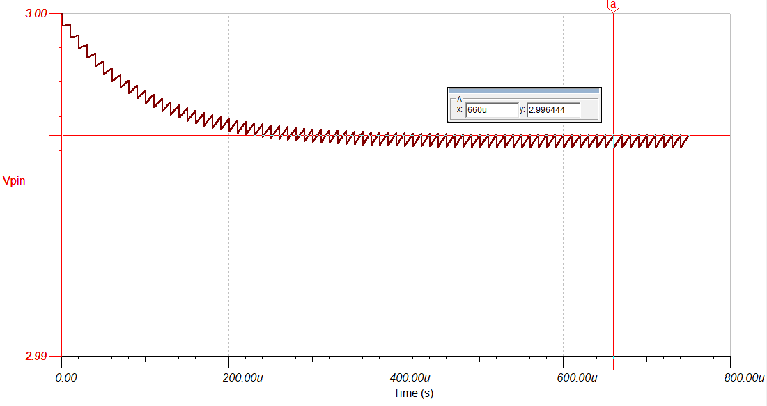
Significant tracking error occurs when the ADC samples too fast relative to the source's ability to recharge Cs through Rs in the time between samples. This is illustrated by simulating the circuit shown in Figure 2-3. The results from the this simulation can be seen in Figure 2-4: each step down in the sawtooth waveform is a charge equalization due to ADC sampling. In this situation, the first sample causes the voltage on the pin to drop by about 0.5 LSBs, resulting in a good sample of the DC input voltage. However, the external source is only able to partially able to recharge Cs before the next sample occurs. Each sample subsequently bleeds off some of the charge on Cs. Eventually, an equilibrium is reached when the delta between the pin voltage and the source voltage increases enough to drive 0.5 LSBs of recovery in the time between samples. In the simulation results of Figure 2-4, the equilibrium is reached at about 3.5mV of tracking error.
 Figure 2-3 ADC Input Circuit With 1 kΩ
Rs and 100 kHz Sample Rate
 Figure 2-4 Simulation Results for 1kΩ
Rs and 100 kHz Sample Rate
Figure 2-4 Simulation Results for 1kΩ
Rs and 100 kHz Sample RateThe settling error target is usually set to 0.5 LSBs, but applications may be able to tolerate more or less settling error. If a 1 LSB settling error target is assumed, the previous example circuit is still far out of target range with 0.5 LSBs of charge-share error plus 3.5mV of tracking error (about 5 LSBs). To get the tracking error within tolerance, either the sample rate needs to be reduced or the source impedance, Rs, needs to be reduced (or both).
Figure 2-5 and Figure 2-6 show that by significantly reducing the source impedance or the sample rate the tracking error can be made to be of a similar magnitude to the error from charge equalization, resulting in an overall settling error within the target of 1 LSBs.
 Figure 2-5 Simulation Results for 100Ω
Rs and 100 kHz Sample Rate
 Figure 2-6 Simulation Results for 1kΩ
Rs and 10kHz Sample Rate