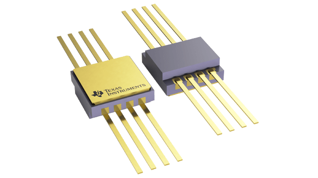
Packaging information
| Package | Pins CFP (HSL) (HKX) | 8 |
| Operating temperature range (°C) -55 to 125 |
| Package qty | Carrier 25 | TUBE |
Features for the SN55HVD233-SP
- QMLV (QML Class V) Radiation Hardness Assured (RHA) MIL-PRF 38535 Qualified, SMD
5962L1420901VXC
- Single Event Latch-up (SEL) Immune to 86 MeV-cm2/mg at 125°C
- Total Ionizing Dose (TID) immune up 50 kRad (Si) at Low Dose Rate
- Qualified over the Military Temperature Range (–55°C to 125°C)
- High-Performance 8-Pin Ceramic Flat Pack (HKX)
- Compatible With ISO 11898-2
- Bus Pins Fault Protection Exceeds ±16 V
- Bus Pins ESD Protection Exceeds ±16 kV HBM
- Data Rates up to 1 Mbps
- Extended –7-V to 12-V Common Mode Range
- High Input Impedance Allows for 120 Nodes
- LVTTL I/Os are 5-V Tolerant
- Adjustable Driver Transition Times for Improved Signal Quality
- Unpowered Node Does Not Disturb the Bus
- Low Current Standby Mode, 200-µA Typical
- Loopback for Diagnostic Functions
- Thermal Shutdown Protection
- Power Up and Power Down With Glitch-Free Bus Inputs and Outputs
- High Input Impedance With Low VCC
- Monolithic Output During Power Cycling
Description for the SN55HVD233-SP
The SN55HVD233-SP is used in spacecraft applications employing the controller area network (CAN) serial communication physical layer in accordance with the ISO 11898 standard. As a CAN transceiver, the device provides transmit and receive capability between the differential CAN bus and a CAN controller, with signaling rates up to 1 Mbps.
Designed for operation in especially harsh radiation environments, the SN55HVD233-SP features cross-wire, overvoltage, and loss of ground protection to ±16 V, overtemperature (thermal shutdown) protection. This device operates over a wide –7-V to 12-V common mode range. This transceiver is the interface between the host CAN controller on the microprocessor, FPGA, or ASIC, and the differential CAN bus used in satellite applications.
Modes: The RS, pin 8 of the SN55HVD233-SP, provides for three modes of operation: high-speed, slope control, or low-power standby mode. The user selects the high-speed mode of operation by connecting pin 8 directly to ground, allowing the driver output transistors to switch on and off as fast as possible with no limitation on the rise and fall slope. The user can adjust the rise and fall slope by connecting a resistor to ground at pin 8, because the slope is proportional to the pin’s output current. Slope control is implemented with a resistor values of 0 Ω to achieve a single ended slew rate of approximately 38 V/µs up to a value of 50 kΩ to achieve approximately 4 V/µs slew rate. For more information about slope control, refer to the Application and Implementation section.
The SN55HVD233-SP enters a low-current standby (listen-only) mode during which the driver is switched off and the receiver remains active if a high logic level is applied to pin 8. The local protocol controller reverses this low-current standby mode when it needs to transmit to the bus. For more information on the loopback mode, refer to the Application Information section.
Loopback: A logic high on the loopback LBK pin 5 of the SN55HVD233-SP places the bus output and bus input in a high-impedance state. The remaining circuit remains active and available for driver-to-receiver loopback, self-diagnostic node functions without disturbing the bus.
CAN bus states: The CAN bus has two states during powered operation of the device: dominant and recessive. A dominant bus state is when the bus is driven differentially, corresponding to a logic low on the D and R pin. A recessive bus state is when the bus is biased to VCC / 2 through the high-resistance internal input resistors RIN of the receiver, corresponding to a logic high on the D and R pins (see Bus States (Physical Bit Representation) and Simplified Recessive Common Mode Bias and Receiver).
