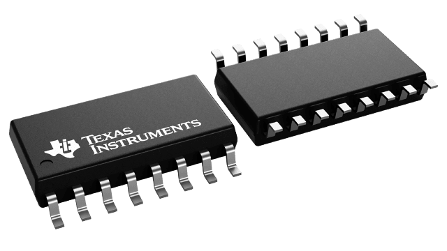
Packaging information
| Package | Pins SOP (NS) | 16 |
| Operating temperature range (°C) -40 to 85 |
| Package qty | Carrier 2,000 | LARGE T&R |
Features for the SN65C1167E
- Meet or exceed standards TIA/EIA-422-B and ITU recommendation V.11
- Operate from single 5V power supply
- ESD Protection for RS-422 bus pins
- ±15kV Human-body model (HBM)
- ±8kV IEC 61000-4-2, Contact discharge
- ±8kV IEC 61000-4-2, Air-gap discharge
- Low supply-current requirements: 9mA maximum
- Low pulse skew
- Receiver input impedance: 17kΩ (Typical)
- Receiver input sensitivity: ±200mV
- Receiver common-mode input voltage range of –7V to +7V
- Glitch-free power-up and power-down protection
- Receiver 3-state outputs active-low enable (SN65C1167E only)
Description for the SN65C1167E
The SN65C1167E and SN65C1168E consist of dual drivers and dual receivers with ±15kV ESD (Human Body Model [HBM]) and ±8-kV ESD (IEC61000-4-2 Air-Gap Discharge and Contact Discharge) for RS-422 bus pins. The devices meet the requirements of TIA/EIA-422-B and ITU recommendation V.11.
The SN65C1167E combines dual 3-state differential line drivers and 3-state differential line receivers, both of which operate from a single 5V power supply. The driver and receiver have active-high and active-low enables, respectively, which can be connected together externally to function as direction control.
SN65C1168E drivers have individual active-high enables.
