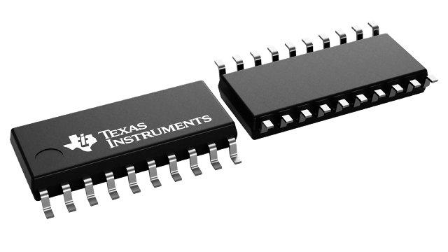
パッケージ情報
| パッケージ | ピン数 SOP (NS) | 20 |
| 動作温度範囲 (℃) 0 to 70 |
| パッケージ数量 | キャリア 2,000 | LARGE T&R |
SN74LS541 の特徴
- 3-State Outputs Drive Bus Lines or Buffer Memory Address Registers
- P-N-P Inputs Reduce D-C Loading
- Hysteresis at Inputs Improves Noise Margins
- Data Flow-thru Pinout (All Inputs on Opposite Side from Outputs)
SN74LS541 に関する概要
These octal buffers and line drivers are designed to have the performance of the popular SN54LS240/SN74LS240 series and, at the same time, offer a pinout having the inputs and outputs on opposite sides of the package. This arrangement greatly enhances printed circuit board layout.
The three-state control gate is a 2-input NOR such that if either G1\ or G2\ are high, all eight outputs are in the high-impedance state.
The 'LS540 offers inverting data and the 'LS541 offers true data at the outputs.
The SN54LS540 and SN54LS541 are characterized for operation over the full military temperature range of -55°C to 125°C. The SN74LS540 and SN74LS541 are characterized for operation from 0°C to 70°C.
