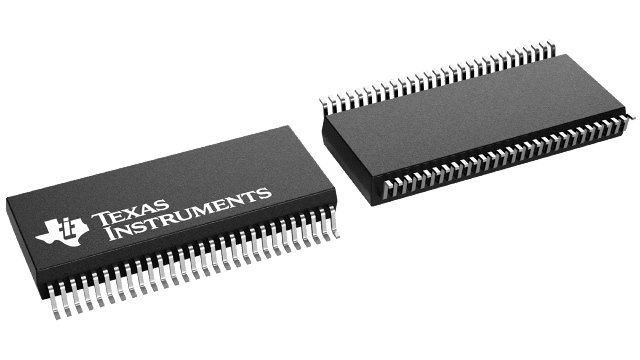
パッケージ情報
| パッケージ | ピン数 SSOP (DL) | 56 |
| 動作温度範囲 (℃) -40 to 85 |
| パッケージ数量 | キャリア 20 | TUBE |
SN74LVT16952 の特徴
- State-of-the-Art Advanced BiCMOS Technology (ABT) Design for 3.3-V Operation and Low-Static Power Dissipation
- Members of the Texas Instruments WidebusTM Family
- Support Mixed-Mode Signal Operation (5-V Input and Output Voltages With 3.3-V VCC)
- Support Unregulated Battery Operation Down to 2.7 V
- Typical VOLP (Output Ground Bounce) < 0.8 V at VCC = 3.3 V, TA = 25°C
- ESD Protection Exceeds 2000 V Per MIL-STD-883, Method 3015; Exceeds 200 V Using Machine Model (C = 200 pF, R = 0)
- Latch-Up Performance Exceeds 500 mA Per JEDEC Standard JESD-17
- Bus-Hold Data Inputs Eliminate the Need for External Pullup Resistors
- Support Live Insertion
- Distributed VCC and GND Pin Configuration Minimizes High-Speed Switching Noise
- Flow-Through Architecture Optimizes PCB Layout
- Package Options Include Plastic 300-mil Shrink Small-Outline
(DL) and Thin Shrink Small-Outline (DGG) Packages and 380-mil
Fine-Pitch Ceramic Flat (WD) Package Using 25-mil Center-to-Center
Spacings
Widebus is a trademark of Texas Instruments Incorporated.
SN74LVT16952 に関する概要
The 'LVT16952 are 16-bit registered transceivers designed for
low-voltage (3.3-V) VCC operation, but with the capability
to provide a TTL interface to a 5-V system environment. These devices
can be used as two 8-bit transceivers or one 16-bit transceiver. Data
on the A or B bus is stored in the registers on the low-to-high
transition of the clock (CLKAB or CLKBA) input provided that the
clock-enable (![]() or
or![]() ) input is low. Taking the
output-enable (
) input is low. Taking the
output-enable (![]() or
or ![]() ) input low accesses the data on
either port.
) input low accesses the data on
either port.
Active bus-hold circuitry is provided to hold unused or floating data inputs at a valid logic level.
To ensure the high-impedance state during power up or power down,
![]() should be tied
to VCC through a pullup resistor; the minimum value of the
resistor is determined by the current-sinking capability of the
driver.
should be tied
to VCC through a pullup resistor; the minimum value of the
resistor is determined by the current-sinking capability of the
driver.
The SN74LVT16952 is available in TI's shrink small-outline (DL) and thin shrink small-outline (DGG) packages, which provide twice the I/O pin count and functionality of standard small-outline packages in the same printed-circuit-board area.
The SN54LVT16952 is characterized for operation over the full military temperature range of -55°C to 125°C. The SN74LVT16952 is characterized for operation from -40°C to 85°C.
