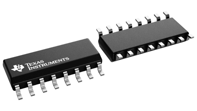
封裝資訊
| 封裝 | 針腳 SOIC (D) | 16 |
| 操作溫度範圍 (°C) -55 to 125 |
| 包裝數量 | 運送業者 2,500 | LARGE T&R |
CD4502B 的特色
- 2 TTL-load output drive capability
- 3-state outputs
- Common output-disable control
- Inhibit control
- 100% tested for quiescent current at 20 V
- 5-V, 10-V, and 15-V parametric ratings
- Maximum input current of 1 µA at 18 V over full package-temperature range; 100 nA at 18 V and 25°C
- Meets all requirements of JEDEC Tentative Standard No. 13B, "Standard Specifications for Description of 'B' Series CMOS Devices"
- Noise Margin (full package-temperature range) =
1 V at VDD = 5 V
2 V at VDD = 10 V
2.5 V at VDD = 15 V - Applications:
- 3-state hex inverter for interfacing IC's with data buses
- COS/MOS to TTL hex buffer
CD4502B 的說明
CD4502B consists of six inverter/buffers with 3-state outputs. A logic "1" on the OUTPUT DISABLE input produces a high-impedance state in all six outputs. This feature permits common busing of the outputs, thus simplifying system design. A Logic "1" on the INHIBIT input switches all six outputs to logic "0" if the OUTPUT DISABLE input is a logic "0". This device is capable of driving two standard TTL loads, which is equivalent to six times the JEDEC "B"-series IOL standard.
The CD4502B types are supplied in 16-lead hermetic dual-in-line ceramic packages (F3A suffix), 16-lead dual-in-line plastic packages (E suffix), 16-lead small-outline packages (NSR suffix), and 16-lead thin shrink small-outline packages (PW and PWR suffixes).
