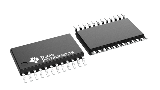
封裝資訊
| 封裝 | 針腳 TSSOP (PW) | 24 |
| 操作溫度範圍 (°C) -55 to 125 |
| 包裝數量 | 運送業者 250 | SMALL T&R |
SN54SLC8T245-SEP 的特色
-
VID V62/22604
- Radiation tolerant:
- Single event latch-up (SEL) immune up to 43 MeV-cm 2 /mg at 125°C
- Total ionizing dose (TID) Radiation Lot Acceptance Testing (RLAT) for every wafer lot up to 20 krad(Si)
- Qualified, fully configurable dual-rail design allows each port to operate with a power supply range from 0.65 V to 3.6 V
- Operating temperature from –55°C to +125°C
- Multiple direction-control pins allows simultaneous up and down translation
- Up to 380 Mbps support when translating from 1.8 V to 3.3 V
- V CC isolation feature that effectively isolates both buses in a power-down scenario
- Partial power-down mode to limit backflow current in a power-down scenario
- Latch-up performance exceeds 100 mA per JESD 78, class II
- ESD protection exceeds JESD 22
- 8000-V human-body model
- 1000-V charged-device model
SN54SLC8T245-SEP 的說明
The SN54SLC8T245-SEP device is an 8-bit non-inverting bus transceiver that resolves voltage level mismatch between devices operating at the latest voltage nodes (0.7 V, 0.8 V, and 0.9 V) and devices operating at industry standard voltage nodes (1.8 V, 2.5 V, and 3.3 V).
The device operates by using two independent power-supply rails (V CCA and V CCB) that operate as low as 0.65 V. Data pins A1 through A8 are designed to track V CCA, which accepts any supply voltage from 0.65 V to 3.6 V. Data pins B1 through B8 are designed to track V CCB, which accepts any supply voltage from 0.65 V to 3.6 V.
The SN54SLC8T245-SEP device is designed for asynchronous communication between data buses. The device transmits data from the A bus to the B bus or from the B bus to the A bus, depending on the logic level of the direction-control inputs (DIR1 and DIR2). The output-enable ( OE) input is used to disable the outputs so the buses are effectively isolated.
The SN54SLC8T245-SEP device is designed so the control pins (DIR and OE) are referenced to V CCA.
This device is fully specified for partial-power-down applications using I off. The I off circuitry disables the outputs when the device is powered down. This inhibits current backflow into the device which prevents damage to the device.
The V CC isolation feature is designed so that if either V CC input supply is below 100 mV, all level shifter outputs are disabled and placed into a high-impedance state.
To put the level shifter I/Os in the high-impedance state during power up or power down, tie OE to V CCA through a pullup resistor; the current-sinking capability of the driver determines the minimum value of the resistor.
