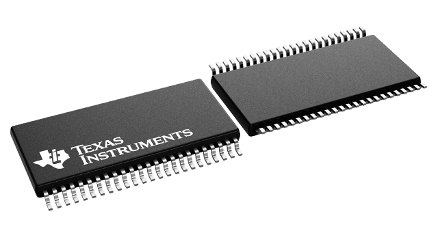
封裝資訊
| 封裝 | 針腳 TSSOP (DGG) | 48 |
| 操作溫度範圍 (°C) -40 to 85 |
| 包裝數量 | 運送業者 2,000 | LARGE T&R |
SN74LV161284 的特色
- 4.5-V to 5.5-V VCC Operation
- 1.4-k
 Pullup Resistors Integrated on All Open-Drain Outputs Eliminate the Need for Discrete Resistors
 - Designed for IEEE Std 1284-I (Level-1 Type) and IEEE Std 1284-II (Level-2 Type) Electrical Specifications
- Flow-Through Architecture Optimizes PCB Layout
- Latch-Up Performance Exceeds 250 mA Per JEDEC 17
- ESD Protection Exceeds JESD 22
- 4000-V Human-Body Model (A114-A)
- 300-V Machine Model (A115-A)
- 2000-V Charged-Device Model (C101)
SN74LV161284 的說明
The SN74LV161284 is designed for 4.5-V to 5.5-V VCC operation. This device provides asynchronous two-way communication between data buses. The control-function implementation minimizes external timing requirements.
This device has eight bidirectional bits; data can flow in the A-to-B direction when DIR is high, and in the B-to-A direction when DIR is low. This device also has five drivers, which drive the cable side, and four receivers. The SN74LV161284 has one receiver dedicated to the HOST LOGIC line and a driver to drive the PERI LOGIC line.
The output drive mode is determined by the high-drive (HD) control pin. When HD is high, the B, Y, and PERI LOGIC OUT outputs are in a totem-pole configuration, and in an open-drain configuration when HD is low. This meets the drive requirements as specified in the IEEE Std 1284-I (level-1 type) and IEEE Std 1284-II (level-2 type) parallel peripheral-interface specifications. Except for HOST LOGIC IN and PERI LOGIC OUT, all cable-side pins have a 1.4-k integrated pullup resistor. The pullup resistor is switched off if the associated output driver is in the low state or if the output voltage is above VCC CABLE. If VCC CABLE is off, PERI LOGIC OUT is set to low.
The device has two supply voltages. VCC is designed for 4.5-V to 5.5-V operation. VCC CABLE supplies the output buffers of the cable side only and is designed for 4.5-V to 5.5-V operation.
