JAJSBW0G December 2012 – June 2019 UCC27531 , UCC27533 , UCC27536 , UCC27537 , UCC27538
PRODUCTION DATA.
- 1 特長
- 2 アプリケーション
- 3 概要
- 4 改訂履歴
- 5 Device Comparison Table
- 6 Pin Configuration and Functions
- 7 Specifications
- 8 Detailed Description
-
9 Applications and Implementation
- 9.1 Application Information
- 9.2 Typical Application
- 10Power Supply Recommendations
- 11Layout
- 12デバイスおよびドキュメントのサポート
- 13メカニカル、パッケージ、および注文情報
パッケージ・オプション
メカニカル・データ(パッケージ|ピン)
サーマルパッド・メカニカル・データ
発注情報
8.3.4 Output Stage
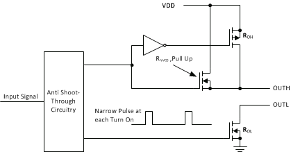
The output stage of the UCC2753x device is illustrated in Figure 39. The UCC2753x device features a unique architecture on the output stage which delivers the highest peak source current when it is most needed during the Miller plateau region of the power switch turn-on transition (when the power switch drain/collector voltage experiences dV/dt). The device output stage features a hybrid pull-up structure using a parallel arrangement of N-Channel and P-Channel MOSFET devices. By turning on the N-Channel MOSFET during a narrow instant when the output changes state from low to high, the gate driver device is able to deliver a brief boost in the peak sourcing current enabling fast turnon.
Split output depicted in Figure 39. For devices with single OUT pin, OUTH and OUTL are connected internally and then connected to OUT.
The ROH parameter (see Electrical Table) is a DC measurement and it is representative of the on-resistance of the P-Channel device only, because the N-Channel device is turned on only during output change of state from low to high. Thus the effective resistance of the hybrid pull-up stage is much lower than what is represented by ROH parameter. The pull-down structure is composed of a N-channel MOSFET only. The ROL parameter (see Electrical Characteristics), which is also a DC measurement, is representative of true impedance of the pull-down stage in the device. In UCC2753x, the effective resistance of the hybrid pull-up structure is approximately 3 x ROL.
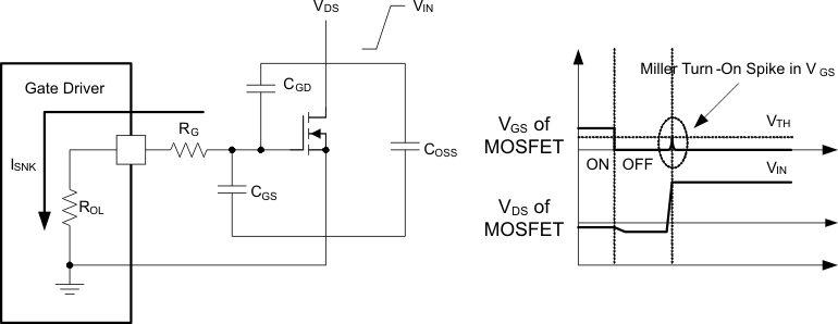
The UCC2753x can deliver 2.5-A source, and up to 5-A sink at VDD = 18 V. Strong sink capability results in a very low pull-down impedance in the driver output stage which boosts immunity against the parasitic Miller turn-on (high slew rate dV/dt turnon) effect that is seen in both IGBT and FET power switches .
An example of a situation where Miller turnon is a concern is synchronous rectification (SR). In SR application, the dV/dt occurs on MOSFET drain when the MOSFET is already held in OFF state by the gate driver. The current charging the CGD Miller capacitance during this high dV/dt is shunted by the pull-down stage of the driver. If the pull-down impedance is not low enough then a voltage spike can result in the VGS of the MOSFET, which can result in spurious turnon. This phenomenon is illustrated in Figure 40.
 Figure 40. Low Pull-Down Impedance in UCC2753x
(Output Stage Mitigates Miller Turn-On Effect)
The driver output voltage swings between VDD and GND providing rail-to-rail operation because of the low dropout of the output stage. In many cases, the external Schottky diode clamps may be eliminated because the presence of the MOSFET body diodes offers low impedance to switching overshoots and undershoots.
